Self-made analog delay pedal using BBD (BOSS DM-3 MOD)
Self-made Guitar Effect Pedals
Explore the articles to learn more about your favorite effect pedals.
|
Building My Own Full Analog Delay Pedal Using BBD
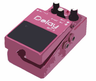 Among guitar effect pedals, analog delay using Bucket Brigade Device (BBD) technology remains very popular. BOSS continues to offer a cool analog delay model as part of their "WAZA" series, which uses three BBD devices to achieve a longer delay time of up to 800ms.
For those interested in building their own delay effect pedal, TONEPAD has published a production article for the "REBOTE Delay," which uses the easy-to-produce one-chip delay IC "PT2399." However, I wanted to take on the challenge of creating my own delay pedal using a more primitive 4096-stage BBD device.
The BOSS DM-2 Analog Delay Uses the Discontinued MN3005
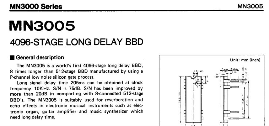 The schematic for the BOSS DM-2 analog delay pedal can be found in its repair service manual. However, the DM-2 uses the Matsushita BBD device "MN3005." This device is no longer manufactured and is hard to obtain. The few available on the market are either very expensive or potentially unreliable used chips taken from abandoned gear.
BBD "MN3205" with Different Specifications is Produced
Currently, the BBD device has been updated to a different specification, the "MN3205." While this device is available for purchase, it is somewhat expensive. Therefore, I decided to use the more affordable Coolaudio "V3205," which is a second-source product of Matsushita's "MN3205."
You can buy the V3205 for around $4, and the accompanying clock generator V3102 costs less than $1.
Difference between BBD devices "MN3005" and "MN3205 (V3205)"
Both of these devices function similarly, featuring a built-in 4096-stage bucket element. However, the new MN3205 (V3205) is designed to operate with a negative power supply. Simply put, the power lines for +9V and GND are reversed compared to the MN3005. Additionally, the maximum power supply voltage for the MN3205 is +9V, which is lower than the +15V maximum of the MN3005. The recommended voltage for the MN3205 (V3205) is +7.5V. Consequently, the power supply circuit of the BOSS DM-2, which uses the MN3005, cannot be used without modification.
Self-Made Pedal Based on the BOSS DM-3 Circuit
Creating my own pedal based on the DM-3, which uses the "MN3205."
BOSS's analog delay DM-2, released in 1982, is a well-known pedal. However, there is also the DM-3, which was sold for a short period following the DM-2. While its functionality is the same as the DM-2, the DM-3 uses the "MN3205" BBD device and supports stereo output. I searched for the DM-3 schematic and found a service manual that includes the schematic using the MN3205.
BOSS effect pedals feature an ON/OFF foot switch that uses FET electronic switches instead of mechanical ones. For my custom delay pedal, I wanted a True-Bypass configuration, so I removed all the FET switches from the schematic, as well as the stereo output.
Circuit diagram (DM-3 modified, PDF)
DM-3's Double Noise Reduction Circuit Provides Excellent S/N Characteristics
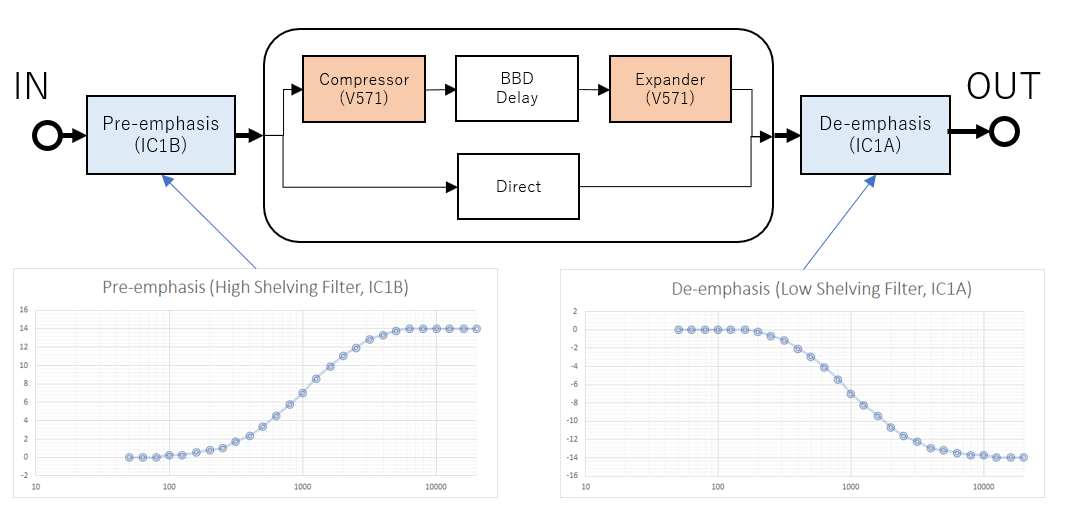
The DM-3 features a double noise reduction circuit that significantly improves signal-to-noise (S/N) characteristics. It includes pre-emphasis and de-emphasis circuits using operational amplifiers for both input and output. To enhance the S/N ratio of the BBD delay section, the treble range is boosted at the input, and then lowered at the output after passing through the delay circuit. This process reduces the high-frequency noise generated in the BBD circuit. Similar technology is used in FM radio broadcasting to improve S/N.
The DM-3 employs a high shelving filter and a low shelving filter using operational amplifiers. The high shelving filter boosts frequencies above 1kHz by up to 14dB (five times the amplitude), and after the delay circuit, the low shelving filter reduces them by 14dB.
Additionally, the delay signal processing involves a compressor and an expander, constructed using halves of a V571 chip before and after the BBD circuit, respectively. This further reduces BBD noise. This setup is similar to the noise reduction technologies like DBX and Dolby used in analog tape recorders. The expander increases the volume only when there is a delay signal and decreases it when there is no delay signal, making BBD noise almost inaudible when no sound is present. Consequently, the DM-3 is a delay effect pedal with low noise and excellent S/N characteristics.
Designing a 2-Layer PCB and Ordering from "Fusion PCB"
This time, I designed a printed circuit board (PCB) and ordered it from "Fusion PCB" in Shenzhen, China, which offers 10 PCBs for $25. I used the freeware "KiCAD" for the entire board design process. I input the circuit diagram, designed the double-sided circuit board, output the standardized board design data (Gerber data), and sent it to "Fusion PCB."
The manufacturing fee is only $5, but DHL shipping costs $20, bringing the total to $25. Even with shipping, it's remarkably affordable to make your own board for $25, a process that would have cost hundreds of dollars a decade ago. The PCBs will arrive in about a week.
10 original printed circuit boards that arrived from Fusion PCB
About Board Design
I designed the PCB using the freeware "KiCAD." First, I input the schematic using the schematic editor and assigned the part shape data, called 'footprints,' to the components. Then, I designed the traces using the board editor. I aimed to fit this analog delay circuit into an MXR-sized enclosure, so I made the board 60mm x 100mm. The actual usable area is smaller because the foot switch area is hollowed out. Designing the traces is relatively straightforward since a double-sided board allows for traces on both the front and back. I connected all the lines except GND, and then filled all remaining areas with a solid ground plane.
Board design requires some experience (I worked for an electronics design company about 25 years ago). There are many books on CAD and board design methods that you can refer to if you want to make your own.
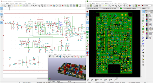
Board design free software "KiCAD"
KiCad PCB Design Data
I have created PCB data using "KiCad (Windows 64-bit) Version: 6.0.4, release build." The ZIP file includes the schematic, board design data, and original component data. Please review the terms of use and disclaimer provided in the attached "readme.pdf" before using this data.
Component Mounting on the Board
I assembled the purchased parts onto the printed circuit board that I ordered based on my design. As a hobbyist who enjoys DIY projects, soldering is the most enjoyable task for me. Despite the challenge of working with numerous parts, I completed the satisfying process of mounting them in about 3 hours.
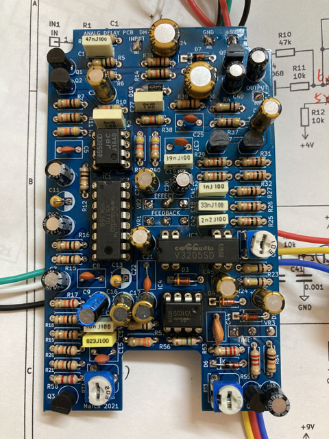
Completed mounting of components on the board
About the Main Parts
For the BBD devices, I used Coolaudio's second-source products "V3205" and "V3102". These are equivalents of the original MN3205 and its clock generator used in the DM-3 analog delay pedal.
The DM-3 employs a noise reduction device known as a compander (NEC uPC1571C). I replaced this with Coolaudio's second-source product "V571".
Regarding transistors for small signals, the original DM-3 uses 2SC1685 and 2SC732. Due to their scarcity, I opted for alternatives "2SC945" and "2SC1815".
The FET "2SK30A" is also challenging to procure, but I managed to find and purchase it. Alternatively, "2SK2880" can be used if the 2SK30A is unavailable.

Coolaudio's second source ICs
Operation Check
"Oops, I made a mistake!"
Upon testing the circuit board on my desk, I encountered an issue. I connected my guitar to the input and routed the output to an amplifier, but instead of hearing my guitar, I heard an oscillating sound. To troubleshoot, I used a small digital oscilloscope recently purchased for $50. I traced the signal from the input and observed it reaching the input operational amplifier (NJM4558DD), but there was no signal coming out from pin 7, the output.
Upon closer inspection of the schematic, I discovered that pins 5 and 6 of the op-amp were mistakenly reversed. With some reluctance, I carefully cut the trace and rewired to correctly connect pins 5 and 6 in their proper positions.
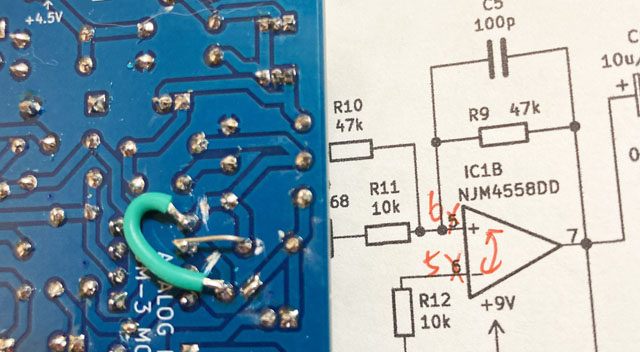
I cut the trace and reconnected it to fix the pin number of the operational amplifier that I made a mistake.
A Delay Sound Came Out!
Upon testing the board, I successfully heard a delay sound. The board includes three semi-fixed potentiometers which I adjusted as follows:
CLOCK Adjustment: This setting determines the maximum delay time. First, I set the RATE potentiometer to achieve the longest delay time possible. Then, I adjusted the CLOCK trimmer. Initially turning it fully to the right maximizes delay time but can introduce aliasing distortion (causing the delay sound to become jerky and muddy). I gradually turned the CLOCK trimmer to the left until the aliasing distortion was minimized to a tolerable level while listening to the delay sound. By design, the maximum delay time is approximately 300ms.
BIAS Adjustment: This adjustment affects distortion. I input a 200Hz sine wave and monitored the output at pin 10 of the compander V571. Gradually increasing the input level, I stopped at the point where either the top or bottom of the sine wave began to clip. I adjusted the BIAS trimmer to minimize distortion, achieving the cleanest sine wave shape possible. If you don't have an oscilloscope, set the effect level potentiometer to maximum, connect it to an amplifier, and adjust the BIAS trimmer to minimize delay distortion audibly.
[Additional Notes] BIAS confirmation with an oscilloscope:
In the lower waveform, the upper (yellow) is the input to the BBD, and the lower (blue) is the output of the V571 (pin 10). It gives a level of input where the output begins to distort. The waveform on the left is distorted at the bottom, but not at the top. This is a condition where the BIAS (center level of the waveform) is too low. The waveform on the right is evenly distorted at the top and bottom. This is the state in which BIAS is appropriate.
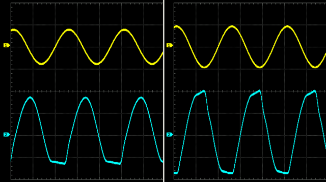
If you lack a signal generator, I used the free Windows software "WaveGene" to generate a 200Hz sine wave signal. The signal from my audio interface, the Steinberg UR22mkII, served as the input for testing this delay.
CANCEL Adjustment: This setting grounds the input. I monitored the output at semi-fixed pin 2 and adjusted the semi-fixed resistor to minimize clock leakage noise in the delay sound. If the input signal is absent, ensure the V571 expander is active to produce delay sound.
[Additional Notes] CANCEL check with an oscilloscope:
When using an oscilloscope, observe the waveform to ensure the outputs of odd-numbered and even-numbered stages are properly connected. Adjust the CANCEL semi-fixed resistor to achieve a balanced and noise-free delay sound.
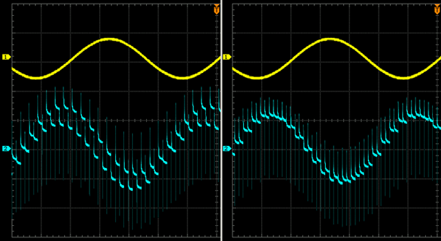

The circuit diagram reveals 4096 bucket elements (capacitors) arranged sequentially within the BBD. These elements switch in pairs (odd and even stages) driven by clock signals (CP1, CP2) of opposite phases. The electric charge stored in these buckets transfers through the stages in a specific order, ensuring the delay effect.
In the waveform examples provided, proper CANCEL adjustment ensures the outputs of odd and even stages are effectively mixed. Poor adjustment may result in clock noise in the final output signal.
Adjust CANCEL with the input turned off using an oscilloscope to align the output at pin 2 of the CANCEL semi-fixed resistor as depicted in the waveform.
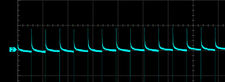
Great to see that the adjustments have resulted in a clear and repeated delay sound!
Built into the Enclosure
Overall Structure
I carefully planned the component placement to ensure the phone jack and foot switch do not interfere with the PCB. I opted for the compact Switchcraft box-type phone jack (#112BX). To create a 20mm clearance between the PCB and other components, I used 2mm thick paper spacers taped inside the enclosure. Unfortunately, due to the PCB's length, there's no space available for a battery.
For the LED indicator, I drilled a 3mm hole and inserted the LED from the inside, securing it with super glue. I opted not to use an LED holder for a cleaner appearance. If you wish to follow a similar approach, please refer to the figure below for guidance.
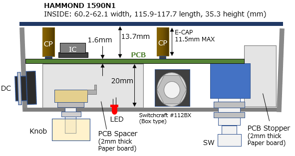
Enclosure Processing
I housed the analog delay circuit in a HAMMOND "1590N1" enclosure painted in blue. The enclosure was processed using a hand drill. Here's the step-by-step process:
1. Positioning: I marked the positions for all components on the enclosure.
2. Drilling: I started drilling with a small pilot hole (1.5mm) at each marked position.
3. Expanding Holes: Next, I enlarged the holes to 3mm using the drill.
4. Final Sizing: Finally, I used a taper reamer to precisely adjust each hole to the diameter required for each component.
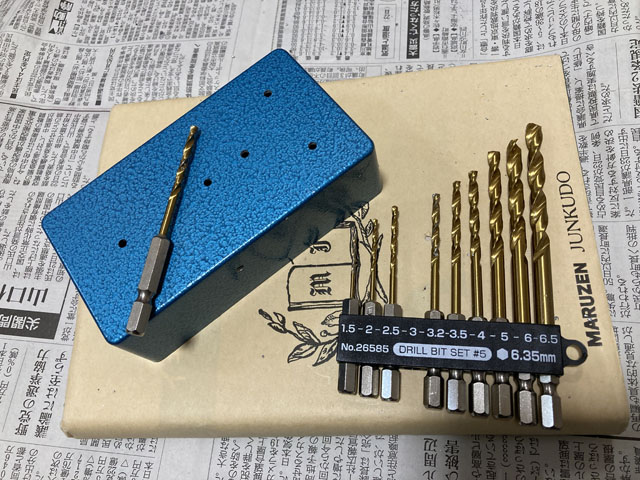
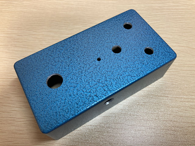
Housing PCB into the Enclosure
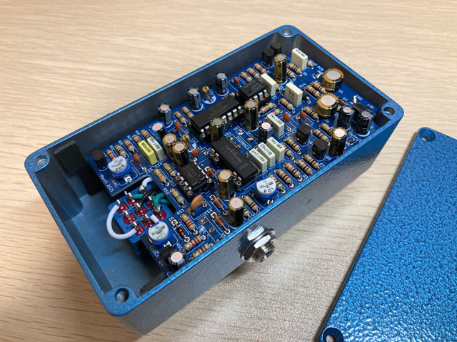
The board width was specifically designed to fit perfectly within the HAMMOND "1590N1" enclosure. I inserted the PCB with the component side facing outward, ensuring a clean and aesthetically pleasing appearance. The input/output jacks and DC jack are positioned near the top of the enclosure to accommodate the PCB.
When the back cover is opened, the overall presentation is neat and resembles a professionally manufactured product. I'm extremely satisfied with how it turned out!
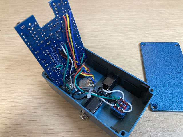
Sound Samples
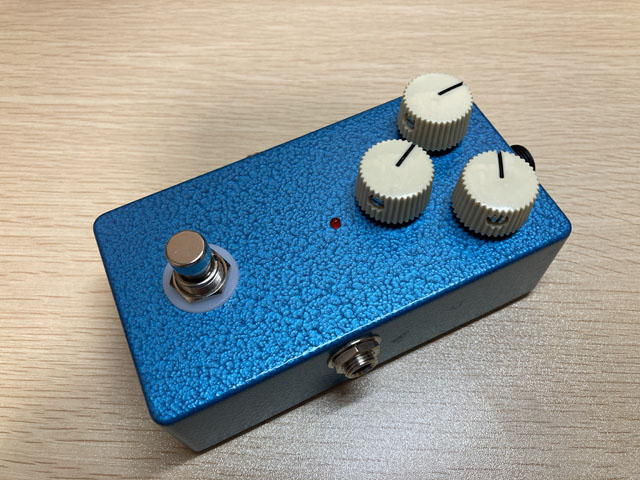
The maximum delay time of my analog delay pedal is set to 300ms. When the FEEDBACK knob is turned up past 2 o'clock, it begins to oscillate. By adjusting the delay time knob during oscillation, I can create a unique oscillating effect characteristic of analog delay pedals. The EFFECT knob functions exactly as I envisioned and performs perfectly.
Below are samples of the delay sound set to the maximum 300ms delay time. You'll hear the distinctive thick and warm analog delay sound that blends seamlessly with the original signal. The repeated feedback gradually distorts and blends, providing a pleasing analog character.
![]() Sample #1: Short chord phrase, 300ms delay (MP3 link)
Sample #1: Short chord phrase, 300ms delay (MP3 link)
![]() Sample #2: Short melody, 300ms delay (MP3 link)
Sample #2: Short melody, 300ms delay (MP3 link)
What I felt after making an analog delay
Music production has evolved from tape recorders to personal computer software like Pro Tools. In today's world, digital technology is prevalent in guitar pedals and amplifiers, often without notice. However, creating an analog delay pedal feels like embracing a nostalgic and timeless aspect of guitar effects.
Electric guitars still use traditional, noisy phone plugs and primitive pickups, which might not seamlessly integrate with modern digital multi-effects devices. Analog delay, with its characteristic high-end roll-off and gradually distorted feedback repeats, embodies the essence of early electric guitar sound?a connection to the instrument's origins dating back to the 1950s, shortly before my own birth. This nostalgic charm extends to effects like spring reverb.
Having played guitar for nearly 45 years and nearing 60, I no longer perform in bands, but I still derive immense joy from playing along with songs by my favorite artists.
For those interested in crafting their own effect pedals, I have created a page explaining tool selection. Please refer to it as a resource for your projects.
[Additional MOD] Added Delay Time Indicator
I recently added an LED indicator to display the delay repeat interval on my analog delay pedal. While this pedal lacks a TAP function and has a relatively short delay time of 300ms, the indicator serves as a personal satisfaction enhancement rather than a practical necessity.
The method involved dividing the clock signal that drives the BBD (V3205), generated by the clock generator (V3102). The V3205, being a 4096-stage BBD, required the clock to be divided by 2048 (half of the clock cycle) to accurately indicate the delay sound's repeat interval.
Given that 2048 corresponds to (2^11), I used a binary counter, specifically the TC4040 with 12 stages, to divide the clock of the V3205. Below is the schematic diagram detailing this modification.
(Click here to see the entire schematic.)
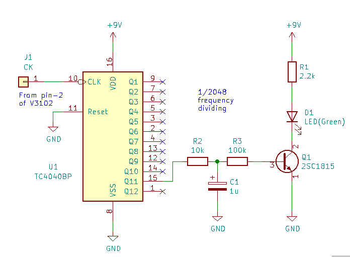
To achieve this, I employed a TC4040 binary counter with 12 stages to divide the clock signal generated by the V3102 clock generator driving the BBD (V3205). Since the TC4040 operates as a CMOS IC and cannot directly drive the LED, I utilized a 2SC1815 transistor for this purpose. Additionally, to mitigate noise at the edges of the blinking LED clock signal, I implemented a time constant circuit (R2 and C1) to ensure the LED lights up gently.
The LED indicator is mounted on a universal board and enclosed in a shield box crafted from aluminum foil tape and vinyl sheet, positioned within the battery compartment of the pedal.
The LED flashes in a pattern resembling a guide for tempo, approximately aligning with quarter notes.
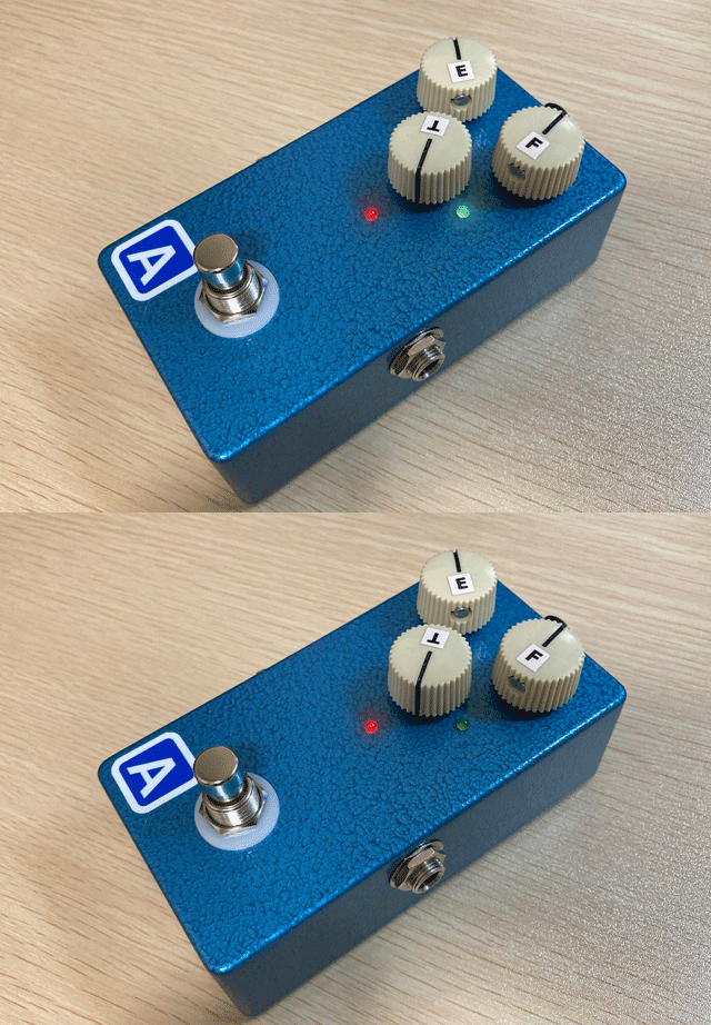
(Visual representation: GIF animation demonstrating the LED blinking pattern.)
[Additional MOD Part 2] Adding BBD for Extended Delay Time of 600ms
I recently extended the delay time of my analog delay pedal by incorporating an additional BBD (V3205). This modification effectively doubles the delay capacity from 300ms to 600ms.
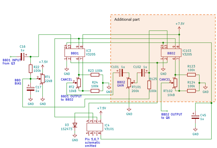
To achieve this enhancement, I utilized the existing clock generator (V3101), which can drive two BBDs in parallel. By connecting another V3205 BBD in series with the original, I doubled the delay time capacity.
In the BBD output stage, I incorporated a mixing pot for odd-numbered and even-numbered stages to blend the outputs properly. Below is the circuit diagram illustrating the configuration of the BBD section:
Circuit Modifications for Extended Delay Time Using Two BBDs
1. Clock Generation and Distribution
Clock Generator (V3101): Provides a stable clock signal to synchronize both BBDs (V3205).
2. BBD Configuration
BBD1 (V3205): Gain Adjustment: Output level adjusted to about +3.5dB higher than input using trimmer RT101.
Bias Adjustment: Bias provided through R125, with DC cut by C102.
BBD2 (V3205): Gain Adjustment: Use semi-fixed resistor to adjust gain to about -3.5dB (approximately x0.64 times relative to input).
Bias Adjustment: Set bias similar to BBD1 using R125 and C102.
3. Gain Adjustment Details
RT101 Trimmer (for BBD1): Adjusts output gain to prevent clipping when inputting to BBD2.
If oscilloscope not available, replace RT101 with 56kΩ and 100kΩ resistors to set appropriate gain.
Semi-fixed BBD2 GAIN Adjustment: Set to approximately -3.5dB using resistors for consistent delay signal level across both BBDs.
4. Biasing Considerations
R125 and C102: Ensure BBD2 receives similar biasing as BBD1 to maintain uniform delay characteristics.
Adjust bias as necessary to optimize delay performance without introducing distortion or noise.
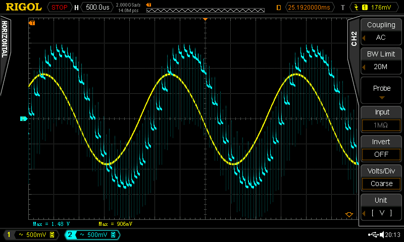
Yellow:BBD1 input (pin.13) / Blue: BBD1 output (pin.2 of RT2 trimmer)
The gain from input to output is about +3.5dB.
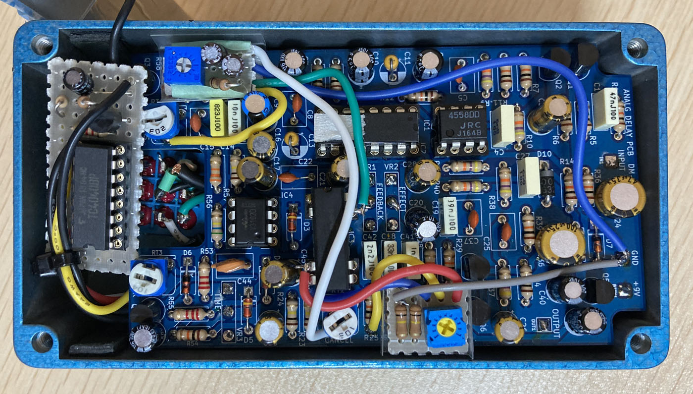
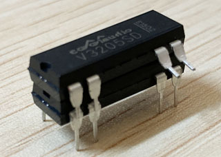
The BBD to be added is taped directly above the original BBD. The pins that connect in parallel to the original BBD are soldered directly, while the other pins are flipped up and wires are soldered to them. Additional parts such as semi-fixed capacitors, resistors, etc., are mounted on a universal board cut into small pieces and attached to the empty area of the printed circuit board with double-sided tape.
Sound Samples with Extended Delay Time
Here are sound samples with a delay time set to approximately 560ms. The original 300ms delay may sometimes interfere with the rhythm due to its short duration, but extending it to nearly 600ms expands its usability.
Using two BBDs doubles the number of stages (buckets), allowing for longer delay times. Doubling the clock frequency fed to the BBDs can achieve the same delay time while reducing folding noise (digital distortion caused by sampling and discretizing), resulting in clearer delay sound.
![]() Sample #1: Short chord, 500ms delay(MP3 link)
Sample #1: Short chord, 500ms delay(MP3 link)
![]() Sample #2: Solo phrase, 500ms delay(MP3 link)
Sample #2: Solo phrase, 500ms delay(MP3 link)
[Additional MOD Part 3] MOD to Enhance Delay Sound Quality
Sampling Frequency and BBD Sound Quality
Similar to how an AD converter in digital circuits samples and converts analog signals into digital values, a BBD samples analog signals and converts them into electric charges stored in its bucket elements to create delay effects. Although the processes differ—digital versus analog conversion—they both involve sampling.
Technically, sampling converts signals from a "continuous system" to a "discrete system," where the maximum frequency handled is limited to half of the sampling frequency, known as the "Nyquist frequency."
For those unfamiliar with the concept, if a BBD samples an input signal at 8kHz (8,000 times per second), its maximum input frequency is limited to 4kHz (half of 8kHz). Inputting a signal higher than this frequency can cause unwanted noise known as "foldback distortion."
The sampling frequency, controlled by the RATE knob on the DM-3, determines how often the BBD samples the input signal. Since the BBD in the DM-3 has 4096 stages fixed, changing the sampling frequency adjusts the delay time.
DM-3 BBD Sampling Frequency
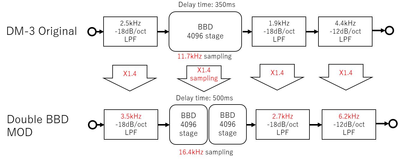
The original DM-3 circuit employs a 4096-stage BBD chip to achieve a maximum delay of approximately 350ms. To calculate the sampling frequency required for this delay time with 4096 stages, we start by determining the time to drive one stage:
(0.35 / 4096) seconds
This time corresponds to the sampling cycle. To convert it to frequency, we take the reciprocal of the cycle time:
1 / (0.35 / 4096)
The calculation results in 11,702 Hz (or 11.702 kHz). Therefore, sampling at approximately 11.7 kHz with a 4096-stage BBD allows for a delay of 350ms.
Low-Pass Filters to Reduce Folding Distortion
The maximum frequency that can be input to the BBD is 5.8 kHz, which is half of the 11.7 kHz sampling frequency determined by the Nyquist frequency principle. Exceeding this frequency threshold introduces folding distortion, rendering the BBD ineffective as a delay circuit.
The DM-3 circuit addresses this with a 2.5 kHz low-pass filter positioned before the BBD. This filter, known as a "third-order Shallen-key filter," attenuates frequencies above 2.5 kHz at a rate of -18 dB per octave. This means that as the frequency doubles, the signal level drops to one-eighth.
You might question whether a 2.5 kHz filter is sufficient, given the 5.8 kHz Nyquist frequency limit. Although this filter doesn't sharply cut off frequencies, its gradual attenuation of -18 dB per octave provides adequate margin. For instance, a 5.8 kHz signal causing fold distortion would be attenuated to -20 dB (one-tenth) after passing through this filter. While some fold distortion may still be perceptible, it remains within practical limits for BBD input.
After passing through the BBD, additional low-pass filters are employed: a third-order 1.9 kHz and a second-order 4.4 kHz filter. These filters are crucial for reducing clock noise mixed within the BBD, as observed in the waveform during CANCEL adjustment. The combined effect of these filters progressively limits the signal to approximately 1.5 kHz or less.
Comparatively, the sound of AM radio extends up to 7.5 kHz, underscoring the restricted frequency response typical of analog delay circuits.
As a result of these design choices, the delay sound of the DM-3 exhibits a round, fluffy quality akin to rolling off the tone knob. This characteristic warmth is a hallmark of analog delay effects.
MOD that raises the frequency of the low-pass filter
To summarize the modification plan for increasing the frequency of the low-pass filters in the DM-3 analog delay circuit:
The primary goal is to enhance the frequency response while maintaining operational stability within the BBD's capabilities.
1. Increased Sampling Frequency:
With the addition of another BBD (V3205) to achieve a maximum delay time of approximately 700ms, the total number of BBD stages becomes 8192 (4096 stages per BBD).
To achieve a delay time of 500ms with 8192 stages:
Sampling frequency = 1 / (0.5 / 8192) = 16384 Hz (16.4 kHz).
This is approximately 1.4 times higher than the original DM-3 sampling frequency of 11.7 kHz.
2. Low-Pass Filter Adjustment:
To accommodate the increased sampling frequency and avoid folding distortion, the cutoff frequency of the low-pass filters before and after the BBDs should be increased by approximately 1.4 times.
For example, if the original cutoff frequency of a filter was 2.5 kHz, it would now be adjusted to approximately 3.5 kHz to 4 kHz.
3. Implementation Considerations:
Modify the capacitor and resistor values in the existing low-pass filters to achieve the new cutoff frequencies.
Ensure that the filters attenuate frequencies above their cutoff points at a rate suitable for maintaining the BBD's integrity and avoiding folding distortion.
Use capacitors and resistors with appropriate values to achieve the desired frequency response without introducing additional noise or signal degradation.
By implementing these modifications, you aim to enhance the high-frequency response of the DM-3 analog delay pedal while maintaining the integrity of the delay effect produced by the BBDs. This approach balances between achieving extended frequency characteristics and preserving the analog warmth and character of the delay sound.
NOTE: The BBD chip divides the internal bucket element into odd-numbered stages and even-numbered stages and drives them with clocks of opposite phases. Therefore, the clock input to the BBD (V3205 pins 2 and 9) is 1/2 of the sampling frequency.
Change the resistance constant of the circuit
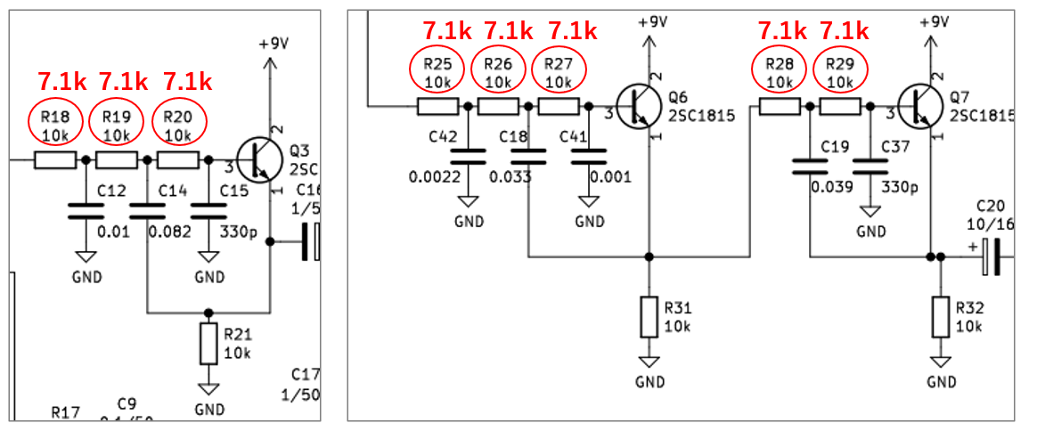
The low-pass filter is a "Shallen-key filter". To increase this cutoff frequency by 1.4 times, I changed the 10 kΩ resistors in series to about 7.1 kΩ, which is 1 / 1.4 times (reciprocal).
Since the printed circuit board I made has a through-hole structure, removing the solder and replacing the resistors is troublesome. Therefore, I soldered a 27 kΩ resistor in parallel with the original 10 kΩ resistor, changing it to 7.3 kΩ.
Frequency Characteristics of the Delay Line after MOD
I measured the frequency characteristics of the delay sound passing through the BBD from the input jack to the output jack. The measurement was conducted by removing R47 (which mixes the direct sound) to isolate the delayed sound.
The signal is nearly unchanged up to 2 kHz, but it starts attenuating beyond 2 kHz and drops to -28 dB (1/25th of the original signal) at 4 kHz. Before the modification, frequencies above 1.4 kHz were significantly attenuated, resulting in a muffled delay sound. This improvement indicates clearer high-frequency response in the delayed signal.
The second analog delay self-made on the surface mount PCB
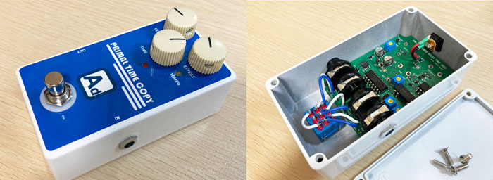
I made a second self-made unit using surface mount components, including modifications. The adjustment pot and phone jack are also mounted on the PCB, imitating the structure of the manufacturer's product. Please see the page below.
NOTE: This document has been improved based on suggestions from ChatGPT.
Language
Self-made
effect pedals
- Pedals list page
 Tool selection
VEMURAM Jan Ray
Xotic BB preamp
Klon Centaur
 Revived old Chorus
 MXR Envelop Filter
 BBD Analg Delay DM-3
 600ms Analog Delay
 Arduino Analog Delay
 BBD Analg Chorus CE-3
CMOS Octaver OC-2
 Riot using chip parts
 Original design noise gate
 EP & MICRO AMP duo
 Keeley 4 Knob Comp
 MXR Phase 90 MOD
 Keeley Blend Comp
 DM-3 longer delay time
 ISP Decimator V2164


