Self-made Suhr Riot clone using surface mounted components
Self-made Guitar Effect Pedals
Explore the articles to learn more about your favorite effect pedals.
|
Surface mount components used for recent effect pedals
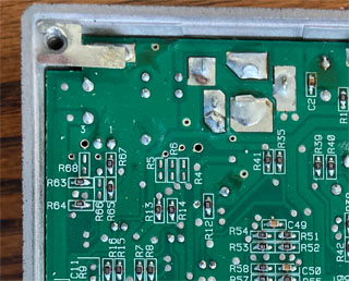 Recent effect pedal PCBs have changed to use surface mount components. In a typical BOSS effect pedal, the size and design of the enclosure have not changed, but the surface-mounted components are used on the PCB. Perhaps it is because the surface mount components are cheaper to manufacture than the larger leaded components. Most digital effect pedals that use DSPs such as digital delay, amp simulator, and digital reverb are made of surface mount components.
Even if resistors, capacitors, operational amplifiers, etc. are changed to surface mount components, the effect on sound will be small. However, with distortion effect pedals, surface mount components may not be available, especially for diodes that significantly change the character of the sound. Surface mount components are not manufactured for germanium diodes such as the "1N34A" that create mellow distortion used in overdrive. Small signal diodes such as "1N914" and "1N4148" used for distortion are available as surface mount components, but I feel that they may affect the sound.
Made a mini-sized "Riot" clone with surface mount components
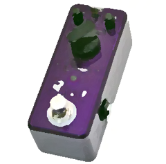 I have made more than 10 analog effect pedals. However, I have never made a small effect pedal that uses surface mount components. I made most kinds of effect pedals, but I have never made a high gain distortion pedal, so this time I decided to make a clone of "Riot" using surface mount components. Looking at the circuit diagram I found on the Internet, it is a relatively simple circuit that uses two operational amplifiers.
I would like to incorporate it into HAMMOND's smallest size (39 x 93 x 31 mm) enclosure "1590A".
Obtain surface mount components online
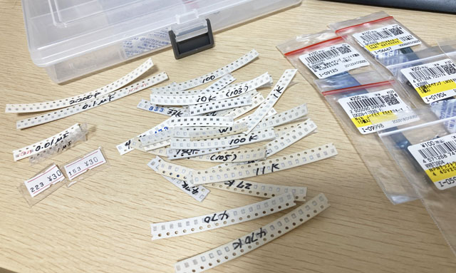
We have made many effectors using surface mount chip parts. The parts I purchased online are summarized on the following page.
Components other than surface mounting
Riot uses small signal diodes, germanium diodes, and LEDs for distortion and switches them. In this PCB, these diodes are all traditional leaded components, not surface mount components. I will mount it upright (hole pitch 2.54 mm) so that it can be made smaller.
This time, I used LEDs for distortion for the first time. It is a bullet-shaped LED with a diameter of 3 mm and a pitch between pins of 2.54 mm. I tried using three cheap red LEDs and one expensive blue diode made by Nichia Corporation.
For other components, I chose the smallest possible components to fit in the enclosure "HAMMOND 1590A" which is only "39 x 93 x 31 mm". In addition, I found and purchased a special "ON-ON-ON" toggle switch on the Internet that switches the diode in three ways.
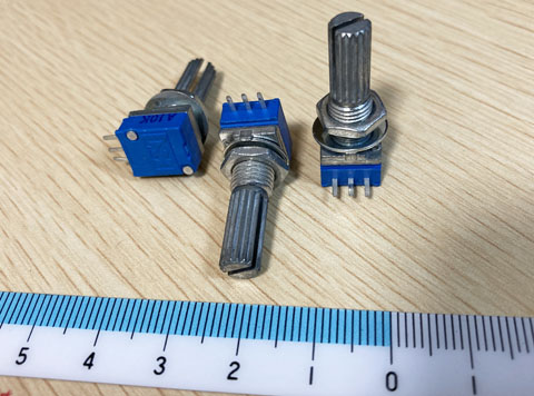
I found and purchased small (10mm x 12mm) pots that can be tightened with screw nuts.
Incorporate into a small enclosure
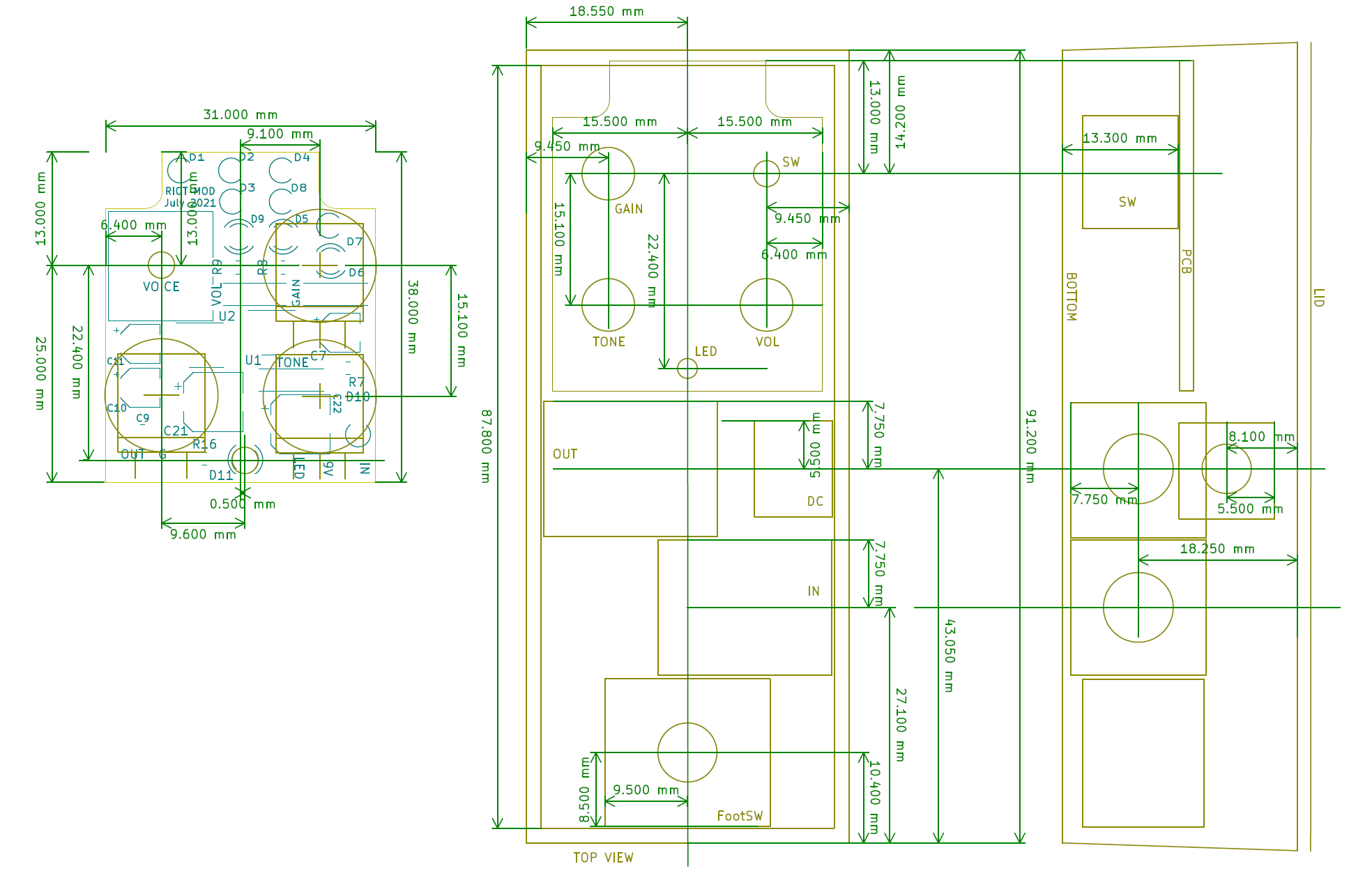
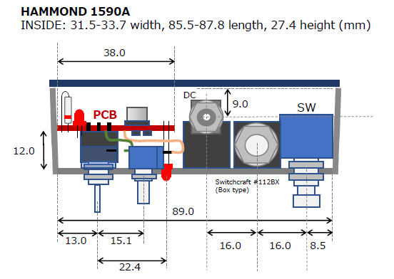
The image when it is housed in the HAMMOND 1590A enclosure is as shown in the figure below. The size of the enclosure is only 31mm in width and 89mm in length, so if a foot switch and input / output jacks are placed, it will occupy more than half of the area. Only about 40mm of space is left for the PCB. Considering the error in the position of the mounting holes, I designed the PCB size at 38mm.
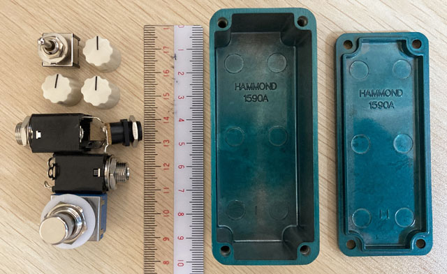
As shown below, I designed the layout of the enclosure using KiCAD's board design editor. If the footswitch and phone jacks are placed together, it will just fit in. It seems necessary to make holes with millimeter accuracy.
Designed a 31mm x 38mm double-sided PCB
Designed with KiCAD
I designed the PCB using the freeware "KiCAD". First, enter the schematic in the schematic editor and assign the part shape data called "footprint" to the used components. Next, design the trace with the board editor.
This time, I mounted a toggle switch that switches the diode on the board, and fixed the board by attaching this switch to the enclosure. I bought the switch at an online shop. Since the manufacturer and model number of the switch were unknown, we decided to create the "footprint" data (data of the outer shape and hole position) by measuring the actual switch after purchase.
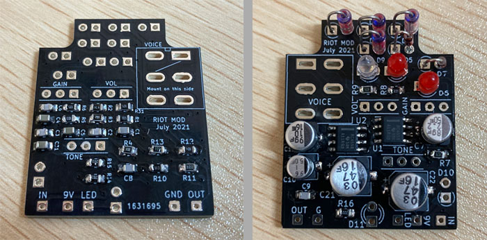
Distorting diodes and LEDs are all ordinary leaded components. These occupy most of the area of the board. I put the short surface mount resistors and capacitors on the back side as much as possible, and the operational amplifiers and the tall electrolytic capacitors on the front side.
The LED for ON / OFF display was mounted on the board, and the head of the LED was exposed from the 3 mm hole of the enclosure.
Since the surface mount components need to be soldered by hand, I chose a part with a large pad for "Hand Soldering" from the KiCAD library.
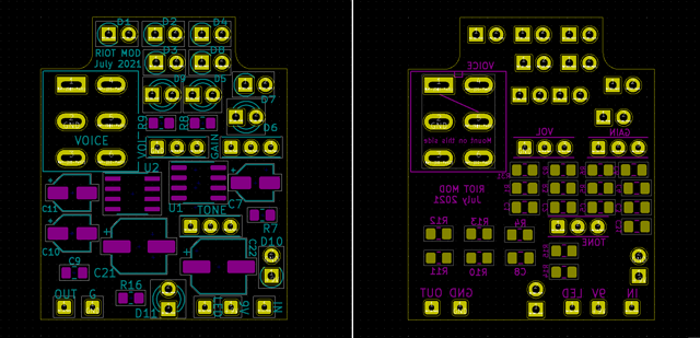
Since it is a two-layer double-sided board, trace can be drawn on the front and back, so trace design is fairly easy. All the lines except GND are connected with a pattern, and all the remaining GND lines are solid earth.
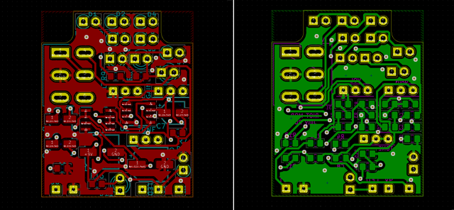
The KiCAD 3D display can be used to see the image of the finished board.
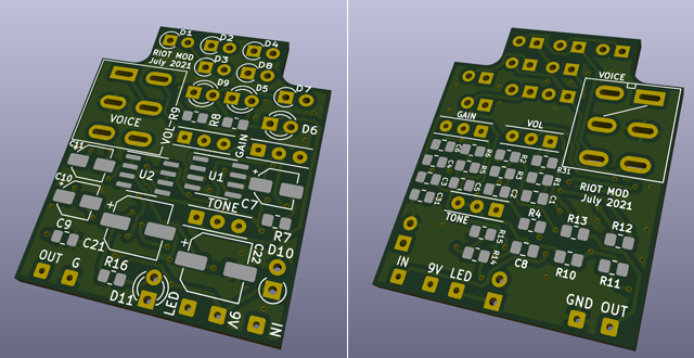
Board design requires some experience (I worked for an electrical equipment manufacturer about 25 years ago), but there are many books on KiCAD and board design methods, so if you refer to it, you can design it.
KiCad PCB design data
The PCB data created using "KiCad (Windows 64-bit) Version: (6.0.4), release build" is provided. The ZIP file contains the schematic, board design data, and original component data. Please read the terms of use and disclaimer in the attached "readme.pdf" before using this data.
Order PCB from "Fusion PCB"
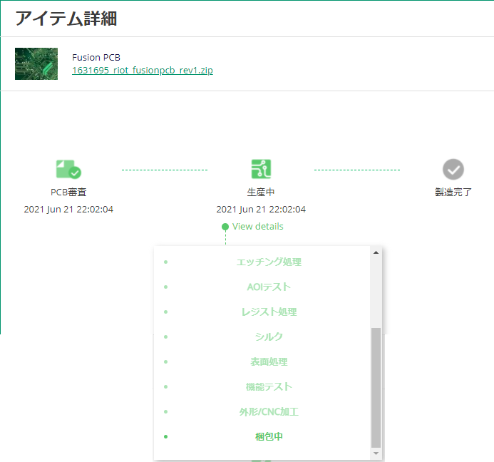 I asked the "Fusion PCB" in Shenzhen, China, which I always use, to manufacture PCBs. I got a $ 5 coupon when I ordered the analog octaver PCB last time, so it's free. I could make it with only $ 19 shipping cost. (I'm worried if "Fusion PCB" is okay.)
This time, I chose the "black" resist color. The manufacturing status of Fusion PCB can be ssen on the WEB page. It usually takes less than two weeks, so I'm looking forward to the completion.
Drilling the enclosure by the time the PCB arrives
Drilling process
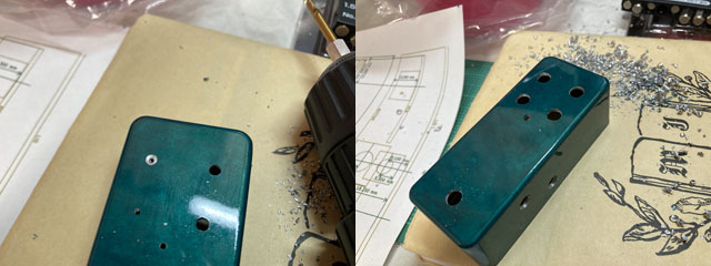
I couldn't wait for the PCB to arrive, so I proceeded with the drilling work. First, plot on the masking tape pasted on the enclosure as shown in the designed figure. Next, make a dent in the center of the hole position with a sharp-edged screwdriver. This is to put the tip of the 1.5mm drill bit used for drilling first on this dent so that the hole position does not shift. This time, the hole position accuracy in mm is required, so I did it carefully.
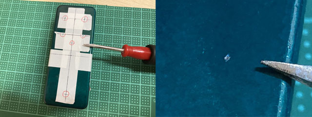
After making dents, remove the masking tape and use drill bits in the order of 1.5 mm, 3 mm, 6 mm to enlarge the hole. As shown in the picture below, I paid attention to the tip of the drill bit so that a 3mm hole would be opened just above the 1.5mm hole. Also, make sure that the LED head fits into the 3mm hole.
Temporarily attach components
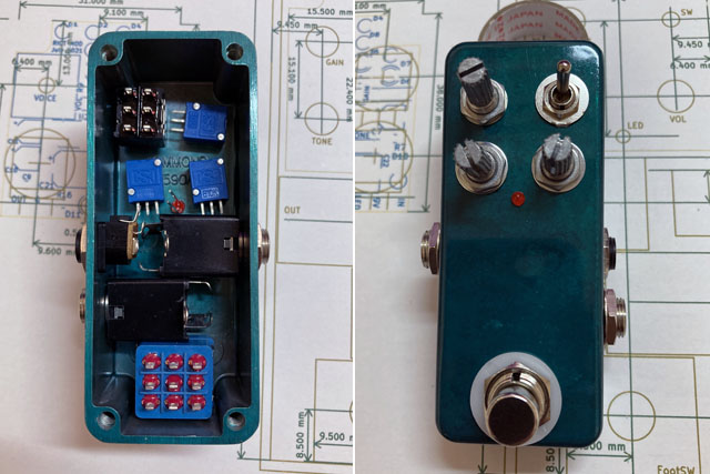
When I temporarily attached the components, I was able to confirm that the components could be installed according to the design drawing. I was also able to see that there was 40mm of space left for the PCB. However, I bent the leads because the DC jack and phone jack leads interfered with each other. Also, since the lead of the pot is long and it is likely to hit the next part, I will shorten it when attaching the wire.
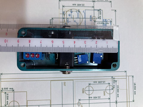
Wire leads to pods using a universal board
I used a universal board to shorten the pod leads and attach the wires.

Board mounting started!
The board ordered from Fusion PCB has arrived
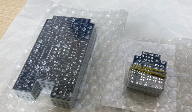
This time, the board arrived about two weeks after the order was placed. As usual, it arrived vacuum packed with bubble wrap. The resist color this time is "black". Compared to the analog delay board ordered at the same time, you can see how small it is.
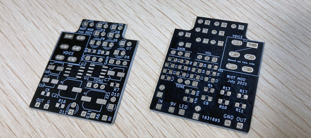
Finished the same as the 3D image of "KiCAD"
Handling of surface mount chip components
Tweezer are required to handle surface mount components. This time, I used 2012 size (2mm x 1.2mm), but I think it feels much smaller than I imagined. The constants are printed on the resistors but not on the capacitors. Therefore, when you take it out of the bag, you need to take it out one by one and put it back in the bag so that it will not be mixed.
The printed constants are difficult to read with the naked eye. I used the magnifying glasses that his wife bought, but I still couldn't read them. I took a picture with my iPhone camera and zoomed in to see it.
The surface mount components are packed in trays and covered with a thin film. I peeled off this film with tweezers and took out the parts in the tray.
Tweezers are required to handle surface mount components
Hand soldering of surface mount parts
I always put the smallest parts first. If you attach the big one first, the tip of the soldering iron will not reach. The order is as follows.
Surface-mounted resistors / capacitors -> Surface-mounted operational amplifiers -> Surface-mounted electrolytic capacitors -> Lead parts such as diodes -> Switches -> Wires
Hand soldering of surface mount components is as follows. This is my first time, so I referred to the video on YouTube. Since I am right-handed, I held the soldering iron in my right hand and the tweezers in my left hand to pinch the parts. The YouTube video recommends applying flux, but as a result the flux contained in the solder was sufficient.

1) Place a small amount of solder on the right side of the pad.
2) Grasp the parts with tweezers and place the parts while melting the piled solder. At this time, make sure that it is placed in the center. If it is misaligned, adjust the position with tweezers while melting the solder.
3) Make sure that the opposite contact of the part is on the left pad.
4) Rotate the board and solder it from the right side to the other pad.
5) Just in case, melt the soldered part again with the tip of a soldering iron and check that it is flowing to the pad.
As a point, even if it is troublesome, you can prevent failure by always soldering from the right side. The amount of solder should be as small as possible. Please be careful not to fill it up. The finish is quite dirty when viewed with magnifying glasses, but don't worry about the details, just think that the terminals of the parts are in contact with the pads on the board.
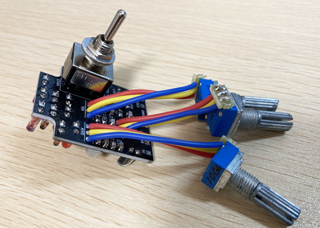
Switch and pot wire mounting
Finally, I soldered the wire connected to the pot and the toggle switch. The wire of the pot was made the minimum length so that a finger could fit under the board when tightening the nut of the pot. When the board is attached, the wires will fold under the board, so I made it as short as possible.
Sound output check
Unfortunately no sound was output
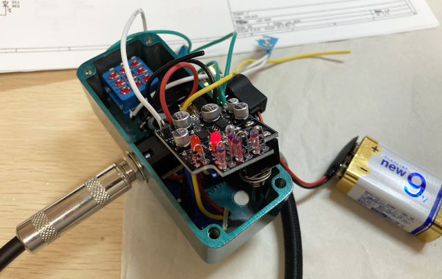
I checked the sound output while temporarily attaching it to the jack of the enclosure. I expected it to be completed, but unfortunately there was no sound. So, I input a sine wave from a personal computer and used my secret weapon, a small oscilloscope, to follow the signal from the input.
As you can imagine, debugging a surface mount component board is difficult because of its small size. It was difficult to just hit the tip of the probe against the pin of the part.
Examining the operational amplifier in the first stage, the signal is coming up to the 3rd pin (+ input), but nothing is output to the 1st pin (output). There was no change even when I turned the GAIN pot, and it felt like the operational amplifier was broken.
After all, it was bad soldering
Since it is difficult to see the soldered state with the naked eye, I took a picture with the iPhone and magnified it. Then, I noticed that the pad of pin 4 (GND) of the operational amplifier was not soldered. There is solder on the 4th pin, but it seems that it did not flow to the pad. For surface mount components, such solder defects may require special attention.
Sound output confirmation OK
After fixing the solder defect, it worked fine. For the first time, I used an LED for the distorted part, but when I tried it, I was surprised that it turned on quite brightly. To turn it on so brightly, a current of about 10mA should be flowing. I reaffirmed the current flowing through the diode.
Sound samples
This is the sound with the germanium diode selected. I am changing the position of TONE. The recording environment is:
Fender Stratocaster (rear humbucker) -> Self-made Riot -> MOOER Preamp006 (Fender blues deluxe clean, cabinet ON) -> UR22mkII -> DAW (Studio One)
![]() Sample: Riot clone, GAIN 12 o'clock, Germanium diode, TONE 12 o'clock (MP3)
Sample: Riot clone, GAIN 12 o'clock, Germanium diode, TONE 12 o'clock (MP3)
![]() Sample: Riot clone, GAIN 13 o'clock, Germanium diode, TONE MAX (MP3)
Sample: Riot clone, GAIN 13 o'clock, Germanium diode, TONE MAX (MP3)
Mini-mini Riot completed
Mounting in the enclosure
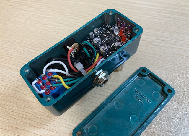
After wiring to the foot switch, I managed to install the pot and toggle switch and completed it. Switches, boards, and jacks were packed tightly. If you make your own mini-sized effect pedal, it may be difficult if the circuit scale is large because there is no space to put the board.
The LED for ON/OFF display was inserted into the hole of the enclosure and its leads were passed through the board. Then I tightened the nut on the toggle switch to fix the board, and finally soldered the LED leads.
I am very happy that it was completed as designed.
Complete with stickers
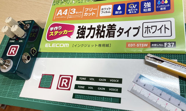
I handcraft a sticker and put it on the top of the enclosure. A picture created with PowerPoint printed on a special sticker paper with an ink jet printer. Sticker paper is made by sticking a transparent sheet on the printed paper, and it is water resistant and durable.
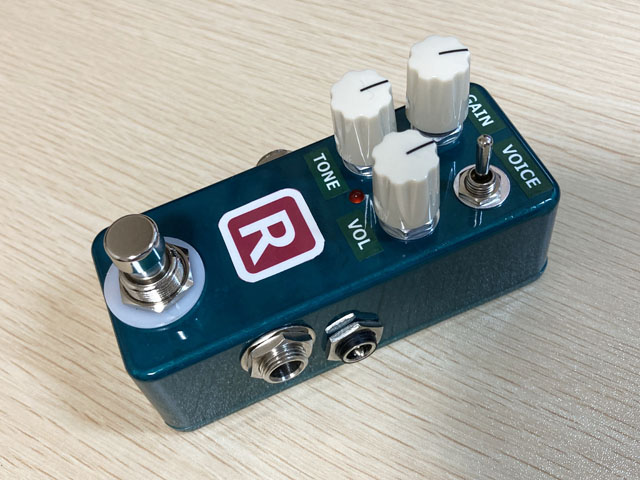
The color of the enclosure is "peacock blue", but it doesn't feel blue, it's more like moss green. I was able to finish it beautifully.
Language
Self-made
effect pedals
- Pedals list page
 Tool selection
VEMURAM Jan Ray
Xotic BB preamp
Klon Centaur
 Revived old Chorus
 MXR Envelop Filter
 BBD Analg Delay DM-3
 600ms Analog Delay
 Arduino Analog Delay
 BBD Analg Chorus CE-3
CMOS Octaver OC-2
 Riot using chip parts
 Original design noise gate
 EP & MICRO AMP duo
 Keeley 4 Knob Comp
 MXR Phase 90 MOD
 Keeley Blend Comp
 DM-3 longer delay time
 ISP Decimator V2164


