ISP Decimator MOD using V2164 VCA self-made report
Self-made Guitar Effect Pedals
Explore the articles to learn more about your favorite effect pedals.
|
Interested in ISP Decimator technology
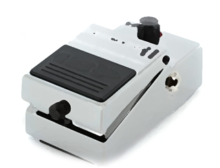 The ISP Decimator is one of the most famous noise reduction pedals for guitars. It seems that it is often used by heavy metal guitar players who use high gain distortion that produces a lot of noise.
I don't play heavy metal music so I don't really need a noise gate pedal, but when I bought a popular and cheap Chinese noise gate pedal and tried it, the sound was great and I was curious about how it worked. When I examined the circuit, I found that it looked like a copy of ISP Decimator. I became more and more interested in Decimator's technology and decided to make it myself.
The ISP Decimator operates as a noise reduction that applies the technology of the expander (the reverse of the compressor) rather than the noise gate that turns the output on and off. It's similar to the technology of DBX and Dolby that existed in the analog tape recorder era.
Decimator's awesome volume control
Volume control by VCA
The device that controls the volume to perform noise reduction operation is the VCA (Voltage-Controlled Amplifier) able to change the sound level by a voltage signal.
Decimator converts the input sound of the guitar into a level signal (envelope), and controls VCA with this signal. When the input sound is loud, the VCA is set to the through state, and when the input sound is low, the VCA level is turned down according to the volume. When the sound becomes quiet, the volume is gradually reduced instead of suddenly reducing the volume to zero. This reduces the unnatural disappearance of the guitar sound when it is attenuated.
Investigate Decimator's VCA control signal generation circuit
Based on the Decimator circuit diagram found on the Internet, I assembled a VCA control signal generation circuit on a breadboard and investigated its operation. Decimator's volume control circuit uses a technology called "Time vector processing" patented by ISP. It is realized by the feedback circuit of the volume correction signal made by two operational amplifiers and a diode.
Normally, to turn an audio signal, such as a guitar input, into an envelope signal, the signal is half-wave rectified with a diode and smoothed with a capacitor. However, due to the hum noise of the guitar or the guitar sound itself, the envelope signal follows the waveform, and when the sound is attenuated, the envelope signal is disturbed up and down (vibrates flutteringly). As a result, the change in envelope becomes jagged, and the attenuation of the sound in VCA becomes rough and unnatural.
Decimator's "Time vector processing" is a awesome technique to improve this unnatural envelope. Two circuits are prepared for smoothing the signal a smoothing circuit with fast tracking (using fast time CR constant) and a smoothing circuit with slow tracking (using slow time CR constant) .By feeding back the correction signal obtained by using differential amplification (subtracting the signal of the slow smoothing circuit from the fast smoothing circuit) to the slow smoothing circuit, it adapts to the fast-following envelope and at the same time smoothes the level signal with a slow tracking time constant. As a result, both the followability to the guitar input and the smoothness when the sound disappears are achieved.
If you are interested, please refer to the figure on page 2 of the ISP white paper. You can find my own explanation in "Schematic and internal operation" below.
VCA device selection
Changed the VCA chip used in Decimator to "V2164"
Looking at the circuit diagram of Decimator found on the Internet, "THAT2181" is used for VCA. The same VCA is used for cheap noise gates in China. However, this IC was not available at mail-order shops in Japan.
A similar VCA device is Coolaudio's V2164, which is commonly used in analog synth VCA modules. This IC can be purchased in Japan at a relatively low price, so I decided to use it.
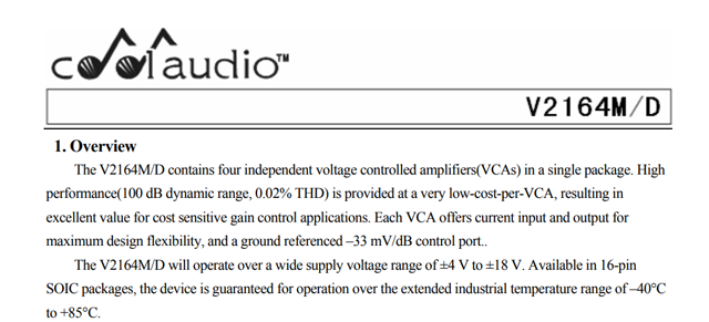
Difference between "THAT 2181" and "V2164"
These VCA ICs operate so that the input and output resistance values change depending on the voltage applied to the control signal pin. In the standard circuit described in the device manual, it is recommended to insert this IC as the input resistance of the inverting amplifier circuit.
The big difference between the two is the direction of the voltage of the control signal. In the case of "THAT2181", the resistance value of input and output "decreases" when the control voltage is increased, while in the case of "V2164", the resistance value "increases" when the control voltage is increased. The operation of the control signals of these two chips is reversed.

Description of the manual of SSM2164 (starting chip of V2164)
In order to generate the control signal for using "V2164", it is necessary to modify the circuit of Decimator.
Two lines of noise reduction
The "V2164" contains four VCA circuits. Decimator's G-String model has a function that can perform noise reduction by inserting a VCA between the send / return of the preamplifier and the power amplifier.
Therefore, I decided to use two of the VCA circuits of the "V2164", one for the guitar input / output and the other for the send / return that follows the input level of the guitar.
I don't use the send / return of a guitar amp, so I'm assuming that I'll use it by inserting it into the line of high gain pedals that have a lot of white noise even when the guitar is silent. Insert this send / return into the switcher loop of the high gain pedals so that the noise reduction is applied only when using the high gain pedal.
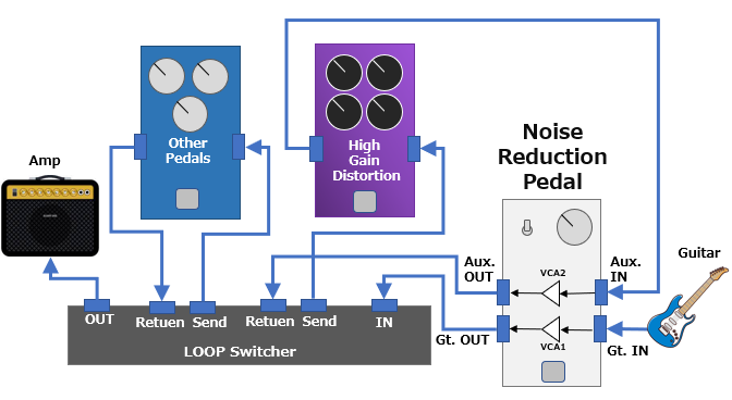
In addition, I added a switch to disable the VCA applied to the first guitar input so that noise reduction is applied only to the high gain pedal, so that it can be used in the same way as the G-String.
Schematic and internal operation
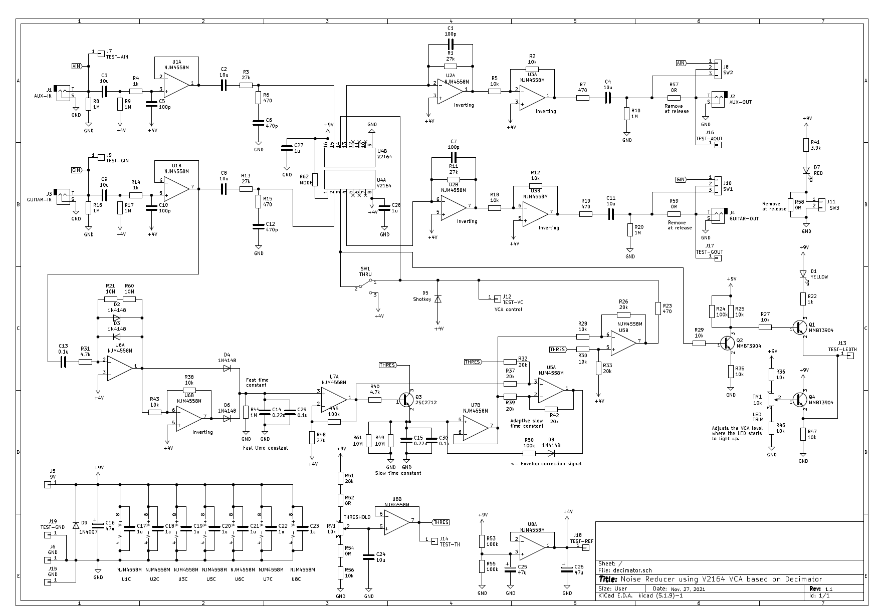
The circuit diagram I made this time is as follows. Some resistors and capacitors are in parallel or in series because they are not available in surface mount components with just the right constants.
The signal is processed as follows: This content is my understanding. It is not officially announced by ISP.
1) Level detection of guitar input
The guitar signal from the input jack passes through the input buffer (U1B) and enters the high gain (+ 72dB) operational amplifier (U6A). If + 72dB is amplified, the operational amplifier will naturally overflow, so there are bidirectional diodes (D2, D3) for feedback, and like the overdrive pedal, the signal is clipped first so that the operational amplifier does not overflow.
The following operational amplifier (U6B) is a phase inversion amplifier. The diode (D4) half-wave rectifies the positive phase waveform from the operational amplifier (U6A). The diode (D6) half-wave rectifies the inverted phase waveform from the inverted operational amplifier (U6B). These are added and full-wave rectification is performed.
After that, there is a capacitor and resistor circuit (R44, C14, C29) as a smoothing circuit (Fast time constant) that quickly follows the input. The electric charge accumulated in this circuit is buffered by the operational amplifier (U7A), and the level signal which follows the input of a guitar quickly is generated.
2) Comparison with threshold level
The generated guitar input level signal (U7A output) is compared to the threshold using an NPN transistor (Q3). The threshold level voltage (THRES) generated by the operational amplifier (U8B) is connected to the collector of the transistor (Q3). This circuit outputs the guitar input level signal to the emitter of the transistor only if the guitar input level signal is less than the threshold level voltage. The collector's threshold voltage limits the guitar's input level signal and adjusts its sensitivity to the guitar's inputs.
3) Time Vector Processing
The operation of ISP's patented "Time Vector Processing" is performed by two operational amplifiers (U7B and U5A). Use an operational amplifier (U5A) to find the difference between the fast smoothing circuit (R44, C14, C29) and the slow smoothing circuit (R61, R49, C15, C30). By adding back the difference (via R50 and D8), the envelope of the guitar level signal is adaptively corrected and smoothed.
This circuit is feedback controlled, so it's difficult to explain how it works. First, obtain the difference (U5A output) by subtracting the voltage of the slow smoothing circuit from the voltage of the fast smoothing circuit. When this difference is smaller than the voltage (C15, C30) accumulated in the slow smoothing circuit (this comparison is made with the diode D8), it operates to remove the charge of the slow smoothing circuit(C15, C30).
As a result, the voltage (C15, C30) of the slow smoothing circuit changes along the envelope of the fast smoothing circuit. Eventually, the followability maintains the time constant of the fast smoothing circuit (R44, C14, C29), while the smoothness of the envelope maintains the time constant of the slow smoothing circuit (R61, R49, C15, C30). In fact the speed of following the guitar input and the smoothness of the sound when it decays are achieved at the same time.
In the circuit diagram of Decimator, the resistance (R61, R49) that determines the time constant of the slow smoothing circuit is 10MΩ. However as a result of trying, I felt that the tracking was too slow, so I reduced it to 5MΩ.
4) VCA control signal generation
The final control signal given to the VCA is generated by the operational amplifier (U5B). Since the VCA "V2164" used has the opposite control voltage direction to the Decimator's "THAT2181", the signal connected to the input polarity (+,-) of the operational amplifier (U5B) is reversed from the Decimator circuit so that the output is reversed. The threshold signal (THRES) added to the operational amplifier is for adjusting the signal level lowered by the threshold level due to the transistor (Q3) in the previous stage.
As a result, when the signal level exceeds the threshold, the gain of VCA becomes full, and when it is below the threshold level, the gain is determined according to the input level, and it operates like an expander.
The generated control signal is input to pins 3 and 14 of the VCA "V2164".
5) VCA circuit
The circuit of VCA "V2164" is the same as the recommended circuit of the device manual. The VCA inputs and outputs are inserted between the negative input resistors (R13) of the inverting amplification operational amplifier (U2B).
Since the phase is inverted by the operational amplifier (U2B), there is an inverting operational amplifier (U3B) to return to the original phase.
6) Level display circuit
The circuit consisting of NPN transistors (Q2, Q1, Q4) is for lighting the LED by following the control signal of VCA. The trimmer (TM1) adjusts the input level at which the LED begins to light. It is used as a guide to see if the VCA is in the through state or in the lowered state. Even if this part is omitted, it does not affect the operation.
Designed with minimal wires, like effect pedal manufacturer products
Mount a pot and phone jacks on a printed circuit board
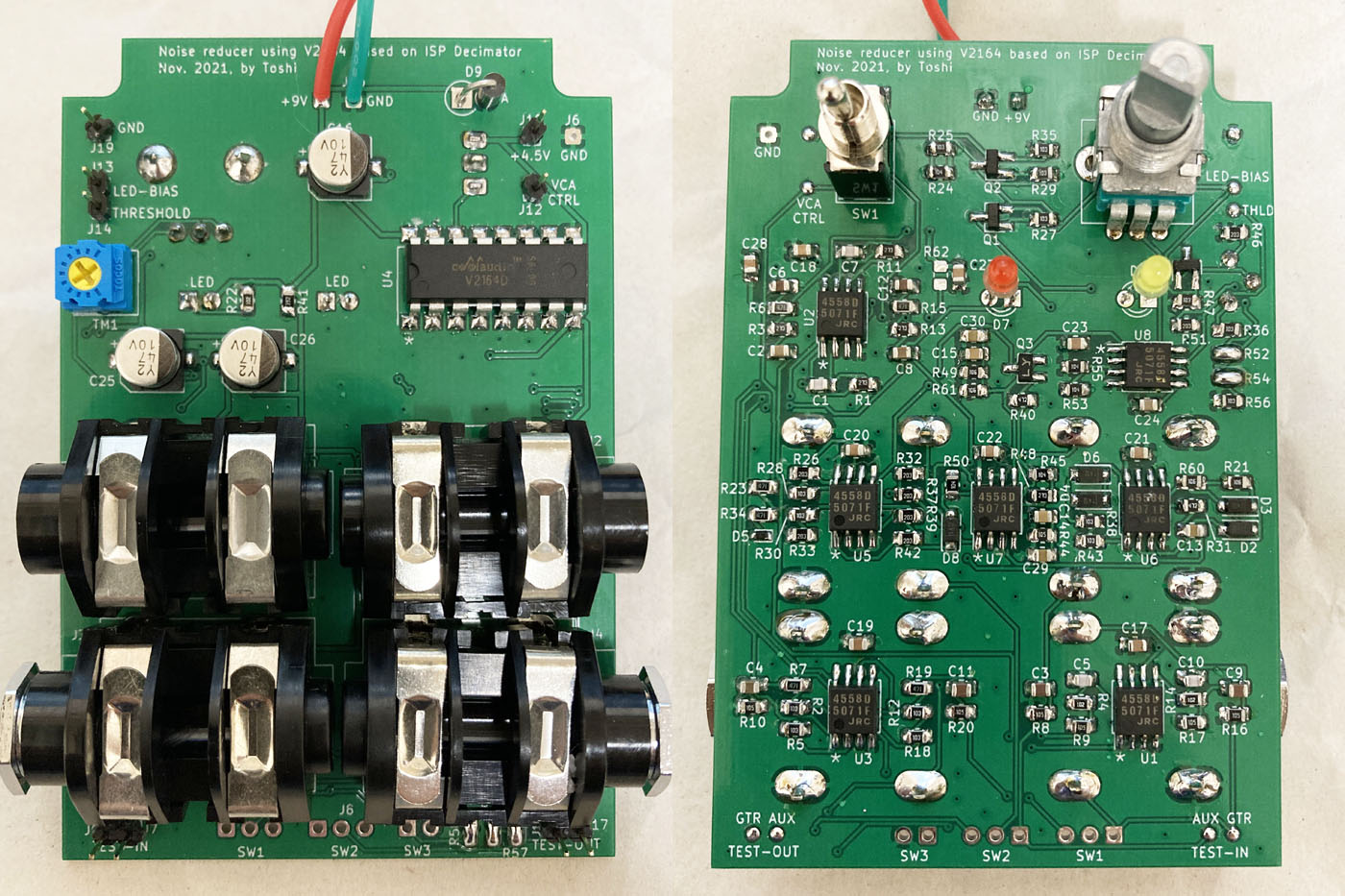
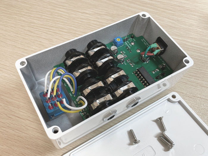
Like the previous "DM-3 BBD longer delay time MOD using surface mount & minimal wiring", I designed it with the minimum wiring inside the enclosure like the products of general effector makers.
A toggle switch, a pot, and an input / output phone jack are mounted on the printed circuit board.
For details on selecting the parts to be used, see the "DM-3 BBD longer delay time MOD using surface mount & minimal wiring" page.

Design surface mount printed circuit boards with KiCAD
I made a printed circuit board on which mounting chip components are mounted. I designed a double-sided printed circuit board using "KiCAD". The pot, phone jack, and surface mount version of the DIP type IC are not available in the KiCAD library, so I created my own footprint (part shape data).
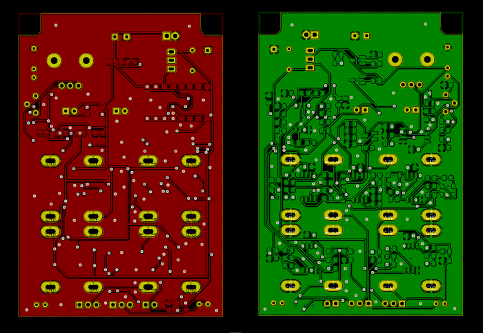
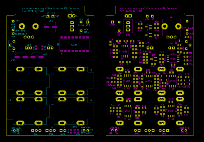
KiCad PCB design data
The PCB data created using "KiCad (Windows 64-bit) Version: (6.0.4), release build" is provided. The ZIP file contains the schematic, board design data, and original component data. Please read the terms of use and disclaimer in the attached "readme.pdf" before using this data.
I ordered the printed circuit board from "PCB go go"
This time, I tried using "PCB go go" from Shenzhen, China, which manufactures within "24 hours". In fact, production was completed in 24 hours, shipped by DHL and arrived in 3 days.
I placed an order at 15:00 on Saturday and arrived the following Wednesday morning.
The quality of the board was perfect, and the silk printing that I was interested in was clearly printed, so there was no problem at all. The manufacturing cost of PCB gogo is $ 5 for 10 sheets. Even including DHL delivery, I was able to produce it for $ 25. The cost of Chinese companies is awesome!
Hand-soldering with chip parts on the board
The surface mount components are really small and require soldering work with tweezers. I'm used to it, but for me with presbyopia, it's pretty tough, but it's also fun.
The 47uF capacitor in the power supply uses electrolysis, but all other capacitors of 1uF or less are multilayer ceramic capacitors that are surface mount components.
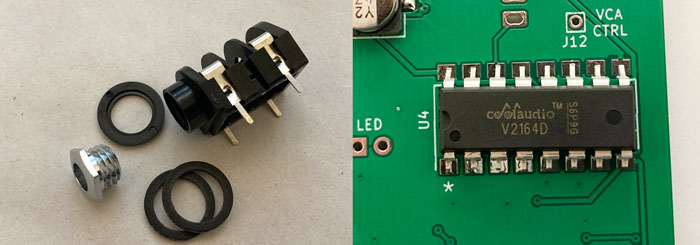
DIP type ICs are surface-mounted by bending the legs sideways and cutting them short. I used pots of board mounting type (RK09L series manufactured by ALPS).
In addition, phone jacks are the board mounting type manufactured by CLIFF as explained above. It must be soldered to fit the inner width of the enclosure. The HAMMOND enclosure is trapezoidally larger by about 2 mm toward the lid, so the jack lead hole is made longer in consideration of the enclosure dimensional error. I inserted the jack into the PCB, put it on the enclosure, decided the position, and then soldered it.
Drilling the enclosure
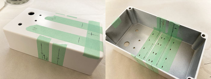
Since pots, LEDs, and jacks are all mounted on the board this time, it is necessary to drill holes accurately according to the position of the parts. To ensure the position, I placed the board on the bottom of the enclosure and marked the hole position with a pen. The height of the jack holes on the side was carefully determined by referring to the height of the pot, the thickness of the board, and the dimensional drawing of the jack.
Once the center position of the part to be attached was decided, the center of the hole was dented with a center punch so as not to shift the hole position, and then a small hole was first drilled around the dent with a 1.2 mm drill. After that, I gradually expanded the holes in the order of 1.5mm, 2mm, 2.5mm, 3mm ... 6mm. After that, I expanded it with a hand-type taper reamer.
The two LEDs were soldered after making a hole in the enclosure. In order to make sure the height is adjusted, I temporarily fixed the pots and jacks to the enclosure with the LED leads passed through the PCB, and after the LED heads came out from the holes in the enclosure, I soldered the LEDs.
PCB operation check
I used the free software (WaveGene) of the PC to generate a sine wave, and I checked the operation using the signal output from the audio interface (Steinburg UR22mkII) used for recording at home.
Unfortunately, it didn't work in one shot, and I followed the cause with an oscilloscope. As a result, the + -polarity of the operational amplifier was incorrect when I wrote the schematic, so I cut the trace of the PCB and reconnected it with a wire. I was able to confirm the exact same operation as when I confirmed the operation on the breadboard.
Response characteristics
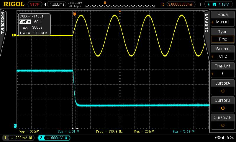
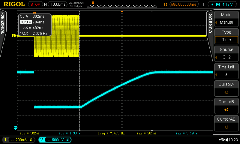
I input a 400Hz sine wave and measured the attack time (level tracking rise time) and release time (time when the level signal returns to the original).
Below is the measured time from the input of a 400Hz sine wave (yellow) to the complete rise of the VCA control signal (blue). It takes 300us (= 0.3ms) for VCA to fully open to 0dB. This time corresponds to one cycle of 3.3kHz. I don't think you can recognize the delay in tracking with the actual guitar sound.
Below is the measured time from turning off the input 400Hz sine wave (yellow) to returning the VCA control signal (blue). It takes about 500ms for the control signal to return to its original state. However, the attenuation factor is -20dB or more when the waveform returns by about half, so you will feel it shorter when you actually listen to it.
Sound samples
These are sound samples of my own noise reduction pedal followed by distortion (BB-preamp, GAIN 2 o'clock).
When using a high gain distortion like Riot on a Strat, the noise is very high. However, when this noise gate is inserted, the distortion sound is cut out, it becomes more powerful, and it feels like the volume has increased.
In case of using guitar output VCA only (send / return VCA is unused)
The recording environment is:
Fender Stratocaster (rear humbucker) -> Self-made noise reduction (VCA1 only) -> Self-made BB-Preamp -> MOOER Preamp006 (Fender blues deluxe clean, cabinet ON) -> UR22mkII -> DAW (Studio One)
The first half is noise reduction OFF, and the second half is ON. You can see the difference more clearly by listening with headphones or earphones.
![]() Sample 1: Short chord (MP3): Sounds like a lump and becomes more powerful.
Sample 1: Short chord (MP3): Sounds like a lump and becomes more powerful.
![]() Sample 2: Solo (MP3): Listen to the first clicks. The last decay is exquisite!
Sample 2: Solo (MP3): Listen to the first clicks. The last decay is exquisite!
![]() Sample 3: Solo (MP3): Excellent followability to the guitar. No noise heard at all.
Sample 3: Solo (MP3): Excellent followability to the guitar. No noise heard at all.
In case of using both guitar output VCA and send/return VCA after hi-gain distortion
The recording environment is:
Fender Stratocaster (middle, single coil) -> Self-made noise reduction (VCA1) -> Self-made BB-Preamp -> Self-made noise reduction (VCA2) -> MOOER Preamp006 (Fender blues deluxe clean, cabinet ON) -> UR22mkII -> DAW (Studio One)
Below is a sample response to picking. Initially, it contains only noise. After that, the same melody is recorded with strong picking and weak picking. When I mute the strings, the noise reduction immediately follows and becomes silent. You will find that there is nothing unnatural about the ability to follow weak picking in the second half.
![]() Sample 4: Solo (MP3): Followability to picking.
Sample 4: Solo (MP3): Followability to picking.
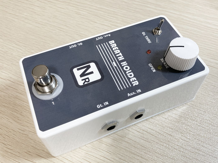
Completed "BREATH HOLDER" by incorporating it into the enclosure
I wanted to make it look like a commercial product, so I put a sticker on the top of the enclosure. I printed a design image made with PowerPoint on sticker paper with an inkjet printer and cut it out. Holes such as pots are cut out according to the holes after sticking a sticker.
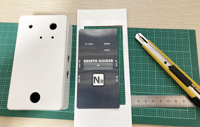
I named it "BREATH HOLDERr" with meaning to keep quiet without breathing when not playing the guitar. I designed the "whole note rest" of the score under the logo in a simple gray color.
Language
Self-made
effect pedals
- Pedals list page
 Tool selection
VEMURAM Jan Ray
Xotic BB preamp
Klon Centaur
 Revived old Chorus
 MXR Envelop Filter
 BBD Analg Delay DM-3
 600ms Analog Delay
 Arduino Analog Delay
 BBD Analg Chorus CE-3
CMOS Octaver OC-2
 Riot using chip parts
 Original design noise gate
 EP & MICRO AMP duo
 Keeley 4 Knob Comp
 MXR Phase 90 MOD
 Keeley Blend Comp
 DM-3 longer delay time
 ISP Decimator V2164


