Full analog 600ms delay pedal with two BBDs
The PCB on this page can be purchased at "Buyee".
You can download the production manual here.
Self-made Guitar Effect Pedals
Explore the articles to learn more about your favorite effect pedals.
|
Production of the third full analog delay pedal using BBD
45 years ago, when I was in junior high school ('78), I started playing the electric guitar, and saved up my pocket money to buy effect pedals such as distortion and compressor pedals. As for the delay pedals, there were only the huge Roland SPACE ECHO (tape type) and the BOSS DM-1, which were too expensive for junior high school students to buy. I still remember the excitement I felt when I used the SPACE ECHO that someone had borrowed for the high school festival.
We can buy digital delay pedals for tens of dollars these days. I have a strong image of a digital delay "adding a sound effect" that is separate from the guitar. On the other hand, I have an image that the analog delay is integrated with the guitar and "creates the sound" of the guitar.
As you can see, I have a strong attachment to analog delays. Therefore, I used two BBDs to create a full analog delay pedal with a delay time of 600ms. This is the third delay pedal I made.
- 1st unit: Through-hole component 300ms analog delay
- 2nd unit: Surface mount component 600ms analog delay
Self-made BBD analog delay pedal specifications
Based on BOSS DM-3 with 2 BBD chips
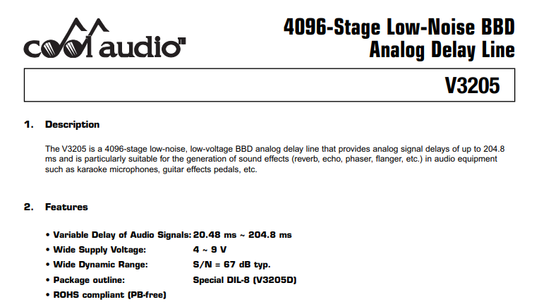 Analog delay pedals typically use a 4096-stage BBD chip. This BBD chip is now a legacy device. The original is Matsushita's MN3005, which is no longer in production. After that, the MN3205 appeared as a successor, but even this chip was discontinued. The chip available in Japan now is a second source product made by Coolaudio.
This time, based on the BOSS DM-3, which provides a maximum delay of 300ms with a single BBD chip, I increased the number of BBDs to two to create a pedal that provides a maximum delay time of 600ms.

Uses through-hole components (THD)
This time, I made my own printed circuit board for general through-hole components (THD). In fact, the second self-made delay pedal was made using surface-mounted (chip) parts, but this time I used through-hole parts, which are simpler than surface-mounted parts. I would like to publish the design data of the printed circuit board I made.
For other detailed specifications, please see the first production article. Explains how noise reduction, pre-emphasis, and low-pass filters work.
- Analog delay pedal using BBD, BOSS DM-3 MOD Self-made report
About the circuit
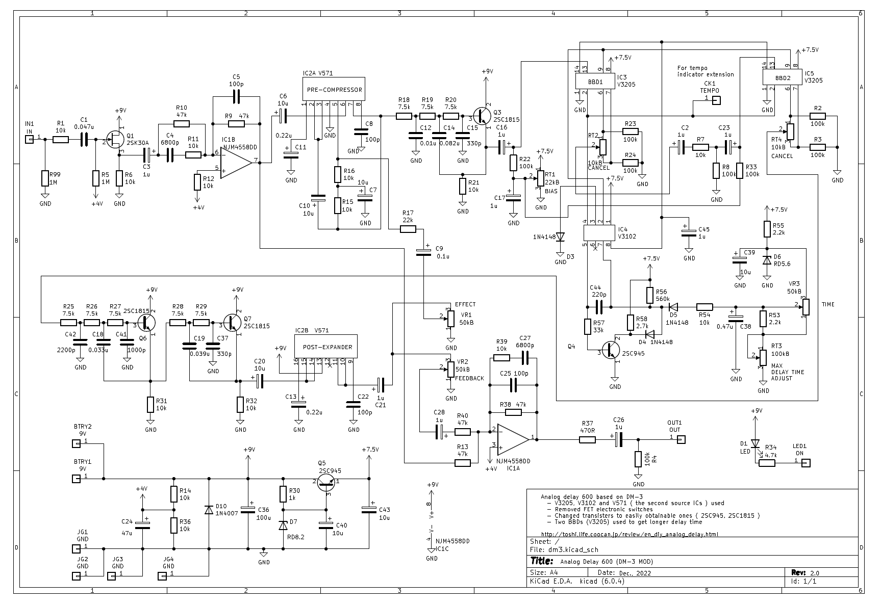
The circuit diagram is shown below. It was written using the free PCB design software "KiCAD 6.0". BBD "V3205" is connected in series to double the delay time. One clock generator "V3102" generates clocks that drive two BBDs.
Resistors (R7/R8, 10k/100k) are inserted between the two BBDs to lower the gain to -2dB. This is because the output is 2dB greater than the input to the BBD.
The circuit also contains an effect ON/OFF LED, which is mounted on the printed circuit board. The switch wiring should be done so that the LED terminal (LED1) drops to GND when the effect is ON.
This delay pedal has a double noise reduction circuit. One is a high-frequency noise reduction circuit using pre-emphasis and de-emphasis, and the other is an S/N improvement circuit using a compander (compressor & expander). Details are explained here.
- Analog Delay 600 Schematic (PDF)
Purchasing parts
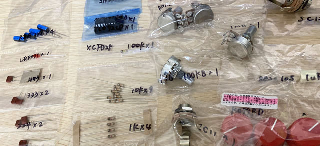
The parts were purchased at "Garrettaudio", a specialty store for effect pedal parts. However, the noise reduction chip "V571" and the semi-fixed resistor (just the right constant) were not available, so I bought these parts at "Akizuki Denshi Tsusho" in Akihabara, Japan's electric town.
Also, the printed circuit board is designed so that the pots can be directly connected to the circuit board, so the three pots have long leads.
Design a printed circuit board with KiCAD
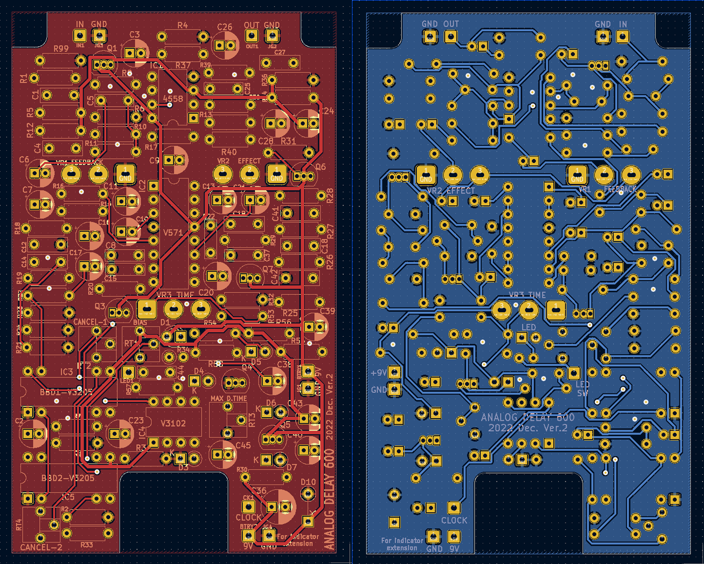
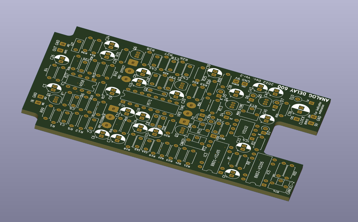
I designed a double-sided printed circuit board using "KiCAD". For the parts that are not available in the standard library, such as the BBD and pot terminals, I created the footprints (part shape data) myself.
KiCad PCB design data
The PCB data created using "KiCad (Windows 64-bit) Version: (6.0.4), release build" is provided. The ZIP file contains the schematic, board design data, and original component data. Please read the terms of use and disclaimer in the attached "readme.pdf" before using this data.
Printed circuit board manufactured by "PCB gogo"
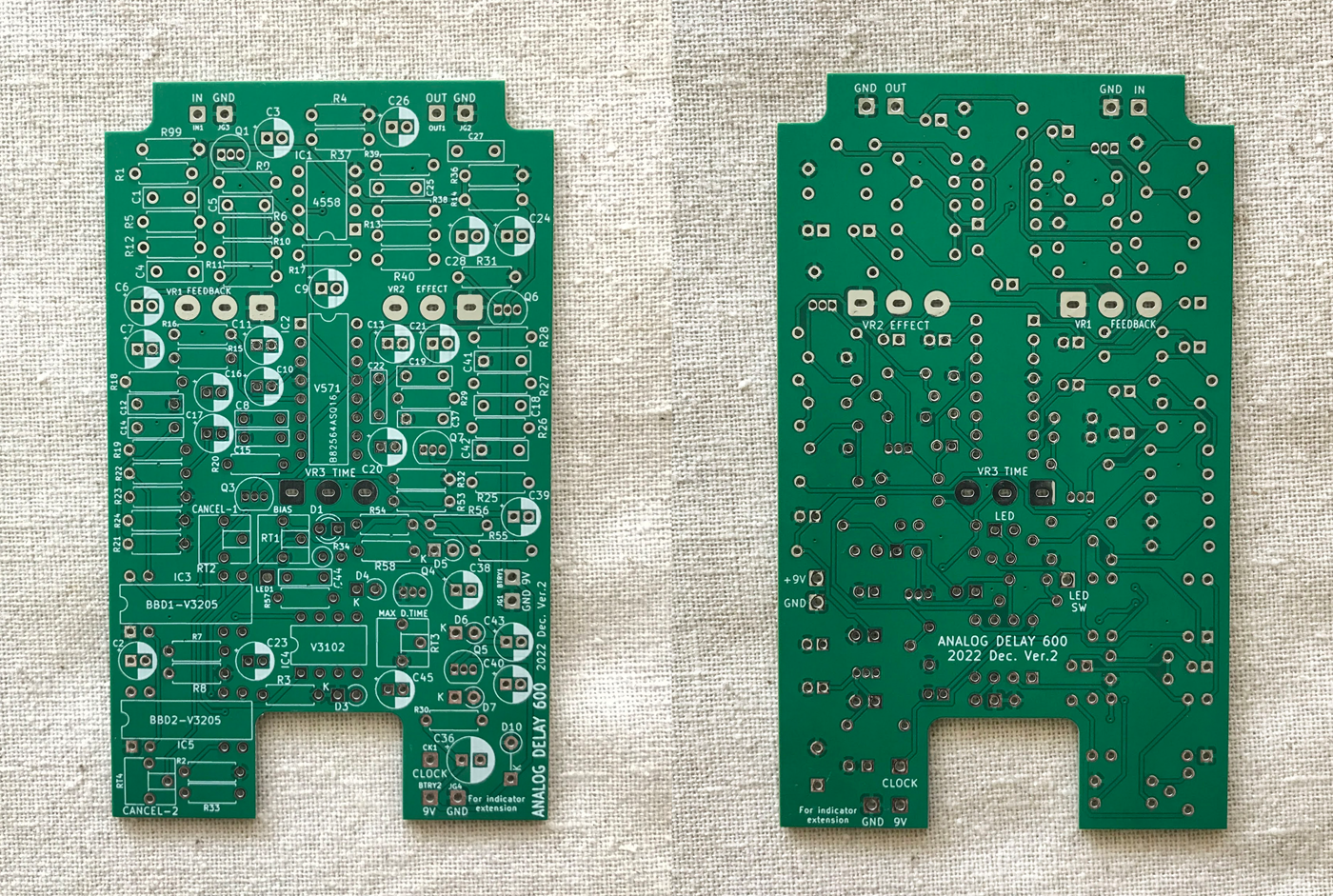
For printed circuit board manufacturing, I placed an order with "PCB gogo", which performs 24-hour express manufacturing at a standard price. It can be created simply by converting the data designed in KiCad into Gerber data and sending it via the web. Including the delivery time of the international courier service (OCS) from Shenzhen, China, it arrived in one week after the online submission. The cost is only $21 including shipping.
Finished PCB
Component mounting on board
Soldering the components is one of the fun parts of making an effects pedal. This time, there are many parts on the printed circuit board, so I was satisfied with making it.
Since the printed circuit board has through holes, it is difficult to remove the parts once they are soldered. I carefully checked constants such as resistors and was careful not to make a mistake.
Arrangement in the case and processing of three pods
This delay pedal uses 3 pots (50kB). When I made the first unit, it was designed to connect the pod to the board with wires, but this time I designed the board so that the terminals of the pot can be directly connected.
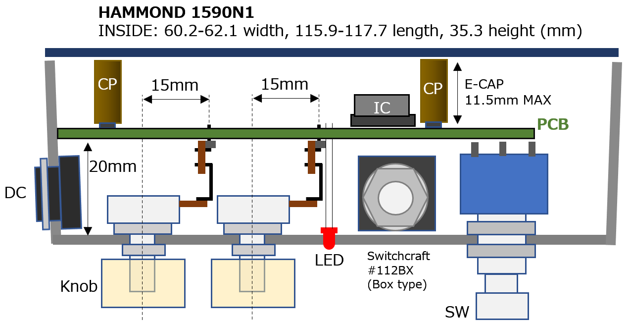
I use HAMMOND's "1590N1" for the enclosure. To fit in this enclosure, you need to place the phone jack between the board and the bottom of the enclosure as shown in the cross section below. Therefore, I attached the pot on the back side of the board and processed the lead of the pot so that there was a space of about 20mm for placing the phone jack.
Specifically, I connected the lead of the pot and the L-shaped pin header with a universal board to make the lead longer. In this production, I used a special pot with long leads that I purchased from Garettoaudio, but I think that it is possible to use a pot with normal lead lengths by extending it with a universal board and an L-shaped pin header.
Enclosure drilling
Assumed placement in enclosure
The installation in the enclosure (HAMMOND 1590N1) assumes the following arrangement. If you use parts up to 11.5mm in height for electrolytic capacitors, you can fit in the height of the pot by setting the height to 20mm. If you don't have enough enclosure height, you can wire the pots together.
Holes suitable for pots and LEDs mounted on the board
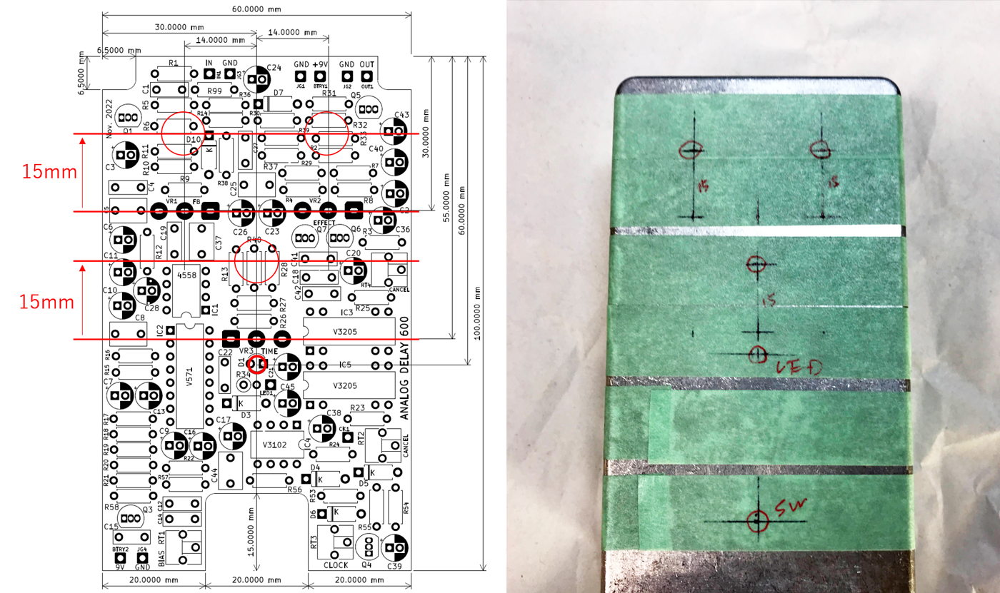
Since the pots and LEDs are mounted on the board this time, it is necessary to drill holes according to the position of the components on the PCB. In particular, the position of the hole in the pot was determined by considering the position of the terminal on the board and the position of the rotating shaft.
The lead-processed pot has a 15mm gap between the lead soldering hole and the rotary shaft of the pot, so I decided the hole position in consideration of this. The LEDs are based on the LED mounting position on the board.
- Tips for drilling holes in the case using a hand drill
I soldered the pots to the board after I finished drilling the holes. First, I temporarily fixed the pots and jacks, checked that the leads of the pots could be passed through the holes in the board, and then soldered the pots.
At this time, I was careful not to touch the jack under the board and the soldering surface on the back side of the board.
In the case of a circuit as large as an analog delay, there are many troubles such as incorrect parts and incorrect wiring. A digital oscilloscope is handy for these troubleshooting.
Operation check
Input test signal
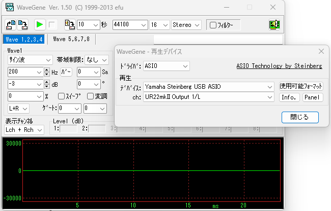
I removed the PCB from the enclosure and used a breadboard to connect the input and output jacks to the PCB and tested. For the test signal, I used free PC software "WaveGene(Japanese ver)" to generate a 200Hz sine wave, output it from the audio interface (Steinberg UR22mkII), and input it to the PCB.
adjustment
CLOCK adjustment
This adjustment determines the maximum delay time. Set the DELAY TIME knob to the longest delay time in advance. Turning the semi-fixed resistor of CLOCK all the way to the right will give the longest delay time, but the aliasing distortion (the delay sound will sound muddy and jerky) will increase. Gradually move it back to the left, and while listening to the delay sound, set it to a point where you can no longer hear aliasing distortion (acceptable to you). The longest delay time is about 500ms.
At the beginning of adjustment, set the CLOCK semi-fixed resistor to 15 o'clock. I think that it is good to do it after adjusting BIAS and CANCEL, which will be described later.
BIAS adjustment
This adjustment determines the input DC offset to a BBD powered by a single supply. If BIAS is out of range, no sound will be produced. First, try setting it in the range of about 11 to 12 o'clock and check that the delay sound is produced.
Turn the effect pot to MAX and plug it into your amp, listen to your guitar, and turn the BIAS to find the spot where the delay distortion is minimal.
[Reference] Check BIAS with an oscilloscope:
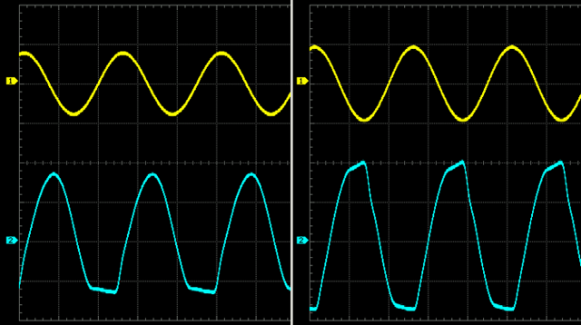
Input a 200Hz sine wave and monitor the output pin 10 of the compander V571. Gradually increase the input level until either the top or bottom of the sine wave clips. Turn the half-fixed BIAS and adjust to the point where the distortion of the sine wave is minimized (where the sine wave shape is clean).
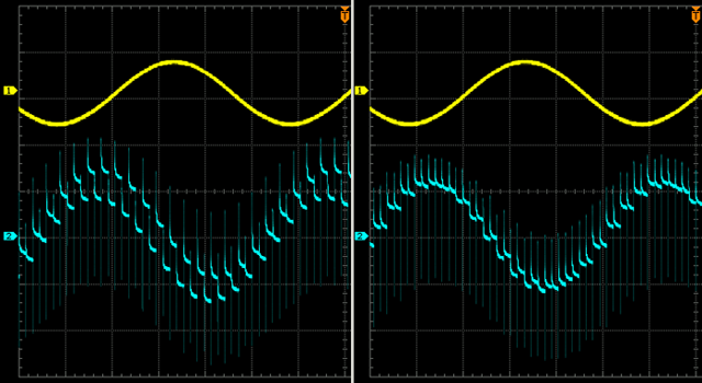
In the waveform below, the top (yellow) is the input to the BBD, and the bottom (blue) is the V571 output (pin 10). A signal is being applied at a level at which the output begins to distort. The waveform on the left is distorted at the bottom but not at the top. This is a condition where the BIAS (mid-level of the waveform) is too low. The right side is evenly distorted up and down. This is the correct condition for BIAS to be centered between the upper and lower thresholds.
CANCEL adjustment (individually for two BBDs)
This is an adjustment to minimize the leakage of BBD drive clock pulses. Each of the two BBDs has separate adjustments.
First, turn the delay time knob to maximum (longest delay). Set the effect pot to MAX, connect it to the amplifier, and turn the CANCEL while listening to the sound. If the guitar input is silent, the V571 expander is closed and the delay sound itself will not come out, so it is necessary to add some input. Turning down the tone of the guitar and inputting a sound that is close to a smooth sine wave makes it easier to hear the outgoing noise. I would recommend using headphones.
The approximate position of the semi-fixed resistor is around 11 o'clock.
[Reference] Confirm CANCEL with an oscilloscope:
In the waveform below, the upper (yellow) is the input to the BBD, and the lower (blue) is the 2nd pin of the CANCEL semi-fixed resistor.

As shown in the circuit diagram above, 4098 bucket elements (capacitors) are arranged in order inside the BBD. Bucket elements are grouped by even and odd numbers, each with a switch driven by the opposite phase clock (CP1, CP2). In accordance with the clock, the charges stored in the buckets are transferred in the order of odd numbered stages -> even numbered stages -> odd numbered stages -> even numbered stages.
In the part that outputs the charge from the last bucket, the even and odd numbers are driven by separate clocks (opposite phase), so the 4097th and 4098th charges are taken out from different pins (OUT1, OUT2). Therefore, it must be connected outside. This is done by mixing with a CANCEL semi-fixed resistor.
The waveform on the left above shows that the CANCEL half-fixed resistor has a poor mixing balance, and the outputs of the odd and even stages are not well connected. In this case, the clock sound will be mixed in the final output. On the right side, the CANCEL adjustment is done correctly, and the outputs of the odd and even stages are well connected.
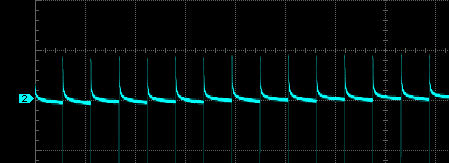
When using an oscilloscope, CANCEL can be easily adjusted by turning the input OFF. At this time, adjust so that the output of pin 2 of the CANCEL semi-fixed resistor is aligned as shown in the waveform below.
* You can see a needle-like pulse in the waveform, but this is reduced by the low-pass filter (2kHz LPF using a transistor) after the BBD, leaving only the sine wave part, so it will not appear in the final output.
Frequency characteristic
Filter measurement of original sound and delay sound
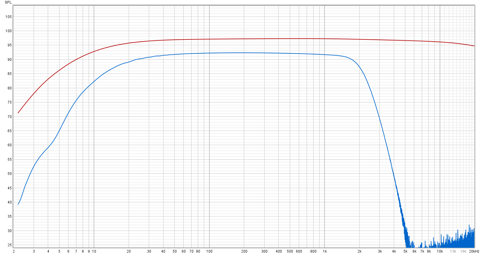
I measured the frequency characteristics using the free measurement software "REW". I measured the frequency characteristics of the direct sound and the delay sound separately. For the direct sound, pre-emphasis is applied at the input operational amplifier, and de-emphasis with the opposite characteristic is applied at the output operational amplifier. The result is a flat characteristic.
Delayed sound is limited to 2kHz by a low pass filter to remove the BBD clock. This characteristic makes the sound of BBD analog delay feel warm.
FFT analysis of delay output
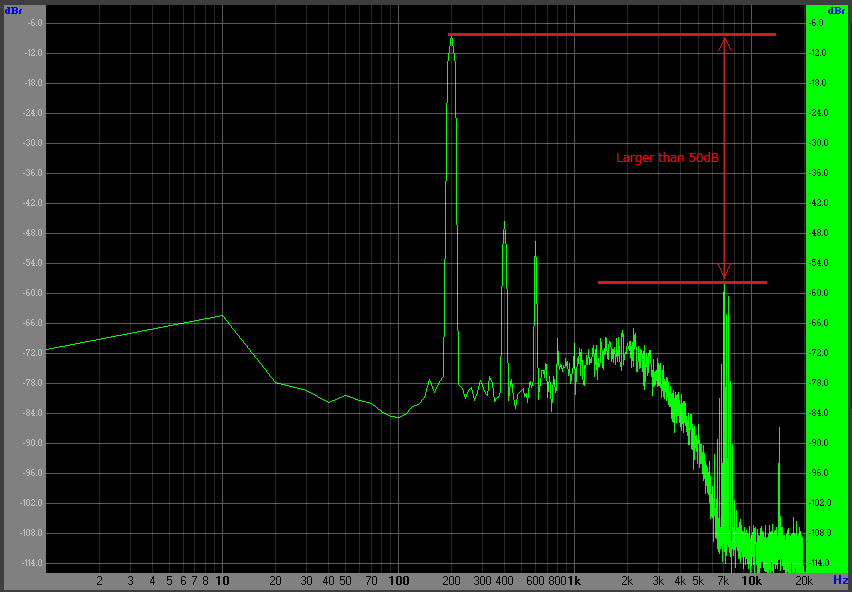
Below is the frequency characteristics of the compander output measured with the free software "Visual Analyzer". Input a 1Vp-p 200Hz sine wave and set the maximum delay time to 570ms. The peak around 7kHz is the leakage of the BBD drive clock. The LPF reduces the noise by more than 50dB, so it is almost inaudible. Shortening the delay time moves the clock to a higher frequency, so the LPF makes it even smaller.
When there is no input, the V571 expander gate closes, so no clock sound is output.
Sound sample
The recording environment is as follows. The delay time is set to the longest (approximately 570ms) and the feedback is set to be long.
In the "high tone" and "low tone" single note samples, you can hear how the repeat sound decays. When the delay time is set to the longest 570ms, a metallic sound like digital aliasing distortion is heard. Below 400ms, this noise is almost unnoticeable.
In the "low tone" sample, the V571's post-expander acts like a noise gate, cutting out only the delayed sound. Even if the repeat sound becomes muddy and noisy, you can recognize that the S/N of the silent part is good.
With “Solo Phrase,” the phrase can be heard clearly even if the delay volume is increased.
Recording environment:
Guitar (Les Paul) -> Self-made noise reduction -> Self-made BB-Preamp (distortion) -> Self-made analog delay (this machine) -> Self-made cabinet simulator -> UR22mkII -> DAW (Studio One)
![]() BBD 570ms Sample: High Tone Single Note (MP3)
BBD 570ms Sample: High Tone Single Note (MP3)
![]() BBD 570ms Sample: Low Tone Single Note (MP3)
BBD 570ms Sample: Low Tone Single Note (MP3)
![]() BBD 500ms Sample: Solo phrase, a lot of delay sound (MP3)
BBD 500ms Sample: Solo phrase, a lot of delay sound (MP3)
Incorporating into an enclosure
To install it in the enclosure, I first installed the phone jack, switch, and DC jack to be placed under the board, and after wiring, I installed the PCB with the pot.
If the guitar is directly connected to the input line, the impedance will be high, making it susceptible to noise. To prevent this, a thin shield wire is used. The outputs are buffered and low impedance so no shielding is required.
Finished with a sticker
For the enclosure, I used a HAMMOND 1590N1 compatible product. Until now, I used the painted one (about $15) and it was expensive, but this time the compatible one (purchased at GarrettoAudio, 70N1) was half the price ($7).
The longest delay time is 600ms, so I named it "ANALOG DELAY 600" and made it a plum color (dark wine red). I designed it with PowerPoint and printed it on a dedicated sticker sheet with an inkjet printer.
It is an unpainted enclosure, but when I put a sticker on it, the retro feel increases and it looks good.
Added delay time indicator function
 I modified the effect ON/OFF LED so that it blinks according to the delay time.
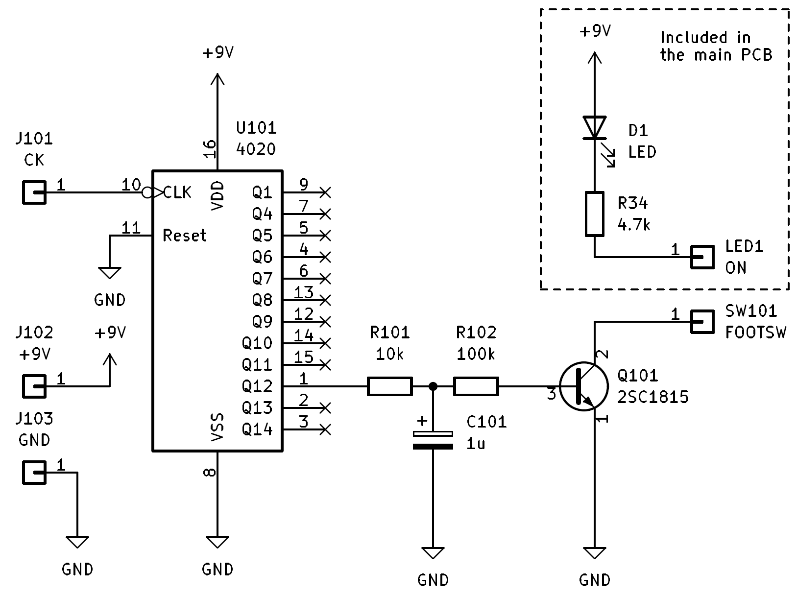
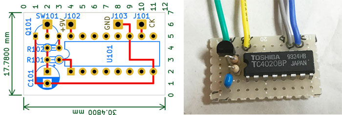
In the circuit that switches ON/OFF with the footswitch, I inserted a circuit that blinks the LED with a pulse generated by dividing the BBD clock by 2048. The schematic is below. It is made with a universal board.
Three self-made analog delay pedals
Left) Analog delay pedal using BBD based on BOSS DM-3
Center) BOSS DM-3 delay time extension mod, surface mount & minimal wiring
Right) This page: 600ms full analog delay pedal with 2 BBDs
Language
Self-made
effect pedals
- Pedals list page
 Tool selection
VEMURAM Jan Ray
Xotic BB preamp
Klon Centaur
 Revived old Chorus
 MXR Envelop Filter
 BBD Analg Delay DM-3
 600ms Analog Delay
 Arduino Analog Delay
 BBD Analg Chorus CE-3
CMOS Octaver OC-2
 Riot using chip parts
 Original design noise gate
 EP & MICRO AMP duo
 Keeley 4 Knob Comp
 MXR Phase 90 MOD
 Keeley Blend Comp
 DM-3 longer delay time
 ISP Decimator V2164


