DM-3 BBD longer delay time MOD using surface mount & minimal wiring
Self-made Guitar Effect Pedals
Explore the articles to learn more about your favorite effect pedals.
|
Modified BOSS DM-3 to get longer delay time of 600ms
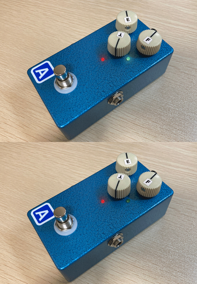 This is the second time I have made a full analog delay using BBD. The first time, I modified the DM-3 circuit to true bypass, added a delay time LED indicator, and added another BBD to double the delay time. The frequency characteristics have been improved by changing the constants of the low-pass filter.
When I first made my own, I designed the printed circuit board with KiCAD for the first time and ordered it from a PCB manufacturer in China. I used a THD component that mounts in a hole in the board. Please see the link below for details on the first DM-3 modified production.
Analog delay using BBD BOSS DM-3 MOD self-made report
This is the second self-made remake using surface mount chip components, including all the first modifications in the circuit.
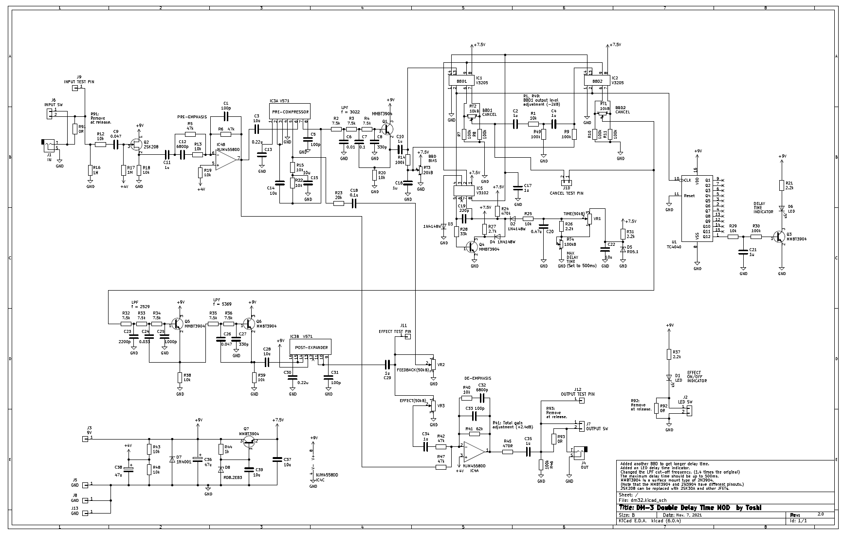
Circuit diagram
In order to outsource the printed circuit board, I entered a schematic into KiCAD that included all the modifications made in the first modified DM-3 production.
Designed with minimal wires like effect pedal manufacturer products
Mounted pot and input/output jack on PCB
Like the products of general effect pedal manufacturers, I mounted a pot and input / output jack on the printed circuit board and designed it to minimize the wiring inside the enclosure.
The DM-3 has three pots (variable resistors). For these, I searched for pots for direct board mounting that are available online. I use a type of part that can be nut-tightened to the case so that it can also be used to fix the board.
If it is difficult to attach the pot directly to the board, or if parts are not available, you can also make it using a universal board and an L-shaped pin header. (Refer to article here.)
As for the input / output jack, I didn't use the type like Switch Craft, which inserts the tip of the jack into the holes on both sides of the enclosure from the inside and nuts it. Once this type is soldered to the PCB, it cannot be inserted into the enclosure hole. Looking at the jacks used in commercial products, it has a structure that is screwed from the outside.
The phone jack with this structure is made by the British manufacturer "CLIFF". I tried using jacks with the model number of "CLIFF S4/MBB/PC-C".
DIP type IC is surface mounted by cutting the legs short
I use Coolaudio's "V3205" and "V3102" for the BBD and clock generator, and Coolaudio's "V750" for the compander IC. However, these ICs are not available in surface mount type packages. If through holls are created on the printed circuit board to mount the DIP type, parts cannot be placed on the back side of the IC. Therefore, I cut the pin of the DIP type IC, bent it, and mounted it on the surface. The binary counter "TC4040" for the delay time LED indicator was mounted in the same way.
BBD2 is attached to the back of BBD1 on the designed PCB. In addition, the binary counter TC4040 for tempo LED display is attached directly behind the clock driver V3102.
Designed surface mount PCB with KiCAD
Again, I made a printed circuit board on which surface mount components are mounted. I designed a double-sided printed circuit board using "KiCAD". Since the surface mount version of the pot, phone jack, and DIP type IC is not available in the KiCAD library, I created the footprint (part shape data) by myself while looking at the actual product.
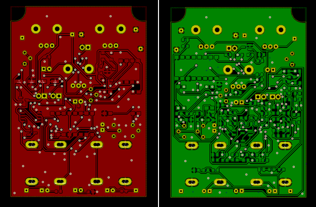
Trace
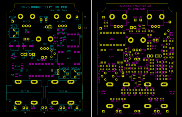
Silk printing
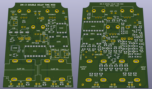
KiCAD 3D image display
KiCad PCB design data
The PCB data created using "KiCad (Windows 64-bit) Version: (6.0.4), release build" is provided. The ZIP file contains the schematic, board design data, and original component data. Please read the terms of use and disclaimer in the attached "readme.pdf" before using this data.
Printed circuit board manufacturing with "PCB gogo"
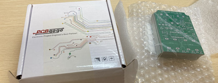
Until last time, I had placed an order to manufacture PCBs from "FusionPCB" in Shenzhen, China, but this time I tried using "PCB go go", which manufactures PCBs within "24 hours". "Fusion PCB" is displayed on the WEB as "Manufactured in 2 to 3 days", but in reality it takes 5 days on average, so it is attractive if the manufacturing time of PCB gogo is true.
The ordering method for PCB gogo is the same as for FusionPCB, just by registering Gerber data. When I placed an order, the production was completed and shipped in 24 hours, which was as expected. However, this time due to the influence of Corona and the influence of China's National Day, it took 6 days from shipping to deliver DHL. I placed an order on Saturday afternoon and arrived the following Saturday morning. The fastest ever!
The quality of the board was perfect, and the silk printing I was worried about was clearly printed, so there was no problem at all.
The cost of manufacturing PCB gogo is $ 5 for 10 pieces, the same as FusionPCB. Even including DHL shipping, I was able to produce it for $25.
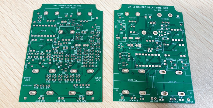
Hand-soldering surface mount components
The surface mount components are really small and require soldering work with tweezers. I'm used to it, but for me with presbyopia, it's pretty tough, but it's also fun.
The 47uF capacitor in the power supply uses electrolysis, but all other capacitors of 1uF or less are multilayer ceramic capacitors that are surface mount components.
DIP type ICs are surface-mounted by bending the legs sideways and cutting them short. I used pots of board mounting type (RK09L series manufactured by ALPS).
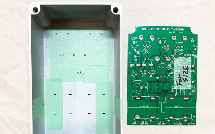
In addition, phone jacks are the board mounting type manufactured by CLIFF as explained above. It must be soldered to fit the inner width of the enclosure. The HAMMOND enclosure is trapezoidally larger by about 2 mm toward the lid, so the jack lead hole is made longer in consideration of the enclosure dimensional error. I inserted the jack into the PCB, put it on the enclosure, decided the position, and then soldered it.
Drilling the enclosure
Since pots, LEDs, and jacks are all mounted on the board this time, it is necessary to drill holes accurately according to the position of the parts. To ensure the position, I placed the board on the bottom of the enclosure and marked the hole position with a pen. The height of the jack holes on the side was carefully determined by referring to the height of the pot, the thickness of the board, and the dimensional drawing of the jack.
Once the center position of the part to be attached was decided, the center of the hole was dented with a center punch so as not to shift the hole position, and then a small hole was first drilled around the dent with a 1.2 mm drill. After that, I gradually expanded the holes in the order of 1.5mm, 2mm, 2.5mm, 3mm ... 6mm. After that, I expanded it with a hand-type taper reamer.
The two LEDs were soldered after making a hole in the enclosure. In order to make sure the height is adjusted, I temporarily fixed the pots and jacks to the enclosure with the LED leads passed through the PCB, and after the LED heads came out from the holes in the enclosure, I soldered the LEDs.
Board operation check
At first, it didn't work. Following the signal from the input with an oscilloscope, I noticed that the transistor footprint specification (pin arrangement) was incorrect when designing the PCB. The transistor is a surface mount component. Forcibly placed the transistor at an angle (Q1 in the lower right photo) and soldered it.
Also, I forgot to put the gain adjustment resistor between BBD1 and BBD2 in the circuit diagram, so I also cut the trace and soldered the surface mount components together (the lower left photo).
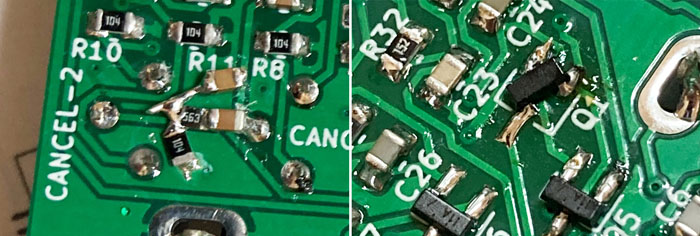
As a result, everything worked fine. When making a printed circuit board, if there are no mistakes in the circuit diagram and component selection on CAD, it can work reliably. I would like to be careful in the next production.
There are adjustments around BBD, but it is the same as the first production, so please see the link below.
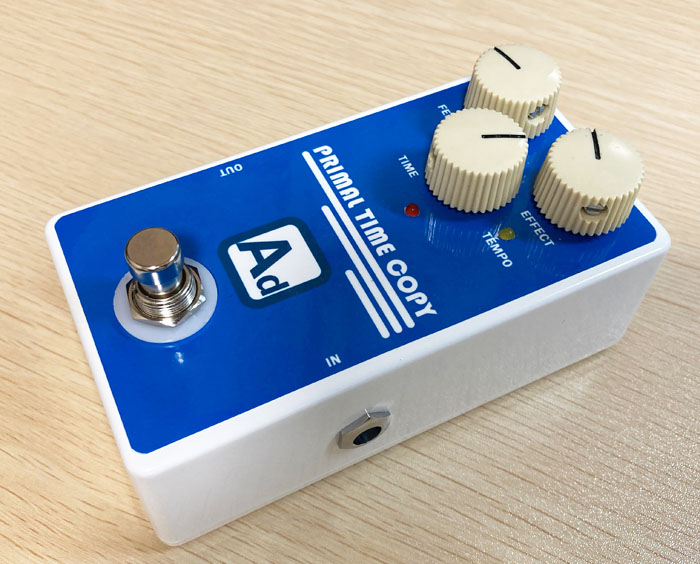
Completed "Primal Time Copy" by putting it in the enclosure
I wanted to make it look like a commercial product, so I put a sticker on the top of the enclosure. I printed a design image made with PowerPoint on sticker paper with an inkjet printer and cut it out. The holes in the pots and switches were cut out to fit the holes after sticking a sticker.
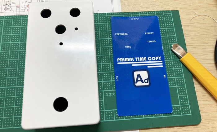
I named it "Primal Time Copy". The name is a combination of the 1980s retro Lexicon digital delay "Prime Time" and MXR "Carbon Copy". Since it was an early analog delay using BBD, I named it with the meaning of "primitive time copier", but I only speak Japanese, so I don't know if it's correct English.
I tried two colors, blue and white. I like it because it has a retro feel.
Comparison with the first self-made
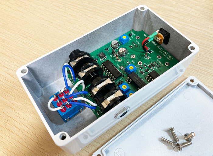
The first self-made delay pedal was made using through-hole parts (THD), and BBD and tempo LED indicators were added later, so the parts are packed tightly. Since the pots and jacks are wired, there is a bundle of wire under the board.
In comparison, this self-made work was impressively refreshing. When checking the operation or performing MOD, if I remove the board, all the parts except the foot switch are attached to the board, so I can easily attach and remove it.
Since both have the same circuit, the sound output is almost the same, but the second pedal sounds less noisy (better S/N). I can't show it in the data because I don't have a noise measuring instrument, but it's probably because there is no bundle of wiring and all the parts are connected in short trace on the PCB.
Language
Self-made
effect pedals
- Pedals list page
 Tool selection
VEMURAM Jan Ray
Xotic BB preamp
Klon Centaur
 Revived old Chorus
 MXR Envelop Filter
 BBD Analg Delay DM-3
 600ms Analog Delay
 Arduino Analog Delay
 BBD Analg Chorus CE-3
CMOS Octaver OC-2
 Riot using chip parts
 Original design noise gate
 EP & MICRO AMP duo
 Keeley 4 Knob Comp
 MXR Phase 90 MOD
 Keeley Blend Comp
 DM-3 longer delay time
 ISP Decimator V2164


